
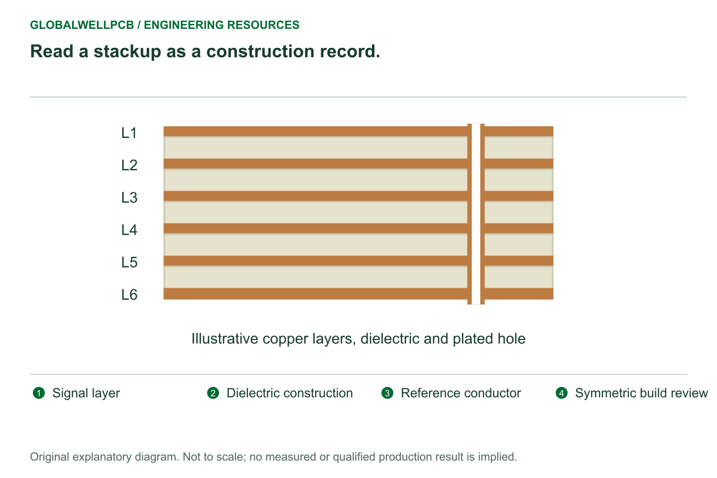
A PCB stackup review should agree the physical construction and the electrical role of every layer before final routing depends on them. Layer count and overall board thickness are insufficient: the design also needs the local dielectric structure, copper definition, reference planes, via spans, and a controlled route for accepting manufacturing changes.
The useful outcome is an agreed build description that the layout engineer, fabricator, and system designer can each interpret. It is an input to detailed design and verification, rather than a promise that the board will meet every electrical or reliability requirement.
Begin with constraints that the stackup must satisfy
Collect mechanical interfaces, component escape needs, electrical requirements, assembly exposure, and any material restrictions before choosing a familiar layer arrangement. A connector may constrain finished thickness. A dense package may constrain interconnect access. An RF path may require a named laminate construction. These constraints can compete, so record which are fixed and which may be revised.
Ask the fabricator for a proposed construction early enough that layout can respond. A drawing that labels dielectric spaces without a buildable material arrangement leaves important choices unresolved. Conversely, accepting a standard construction without checking the product’s constraints can transfer a manufacturing convenience into an unintended design rule.
Keep the first review small and decision focused. Identify the board regions and interfaces that are most sensitive to construction changes, and make those the first subjects for discussion. The goal is to prevent late redesign, not to collect a large table of unused material properties.
Give each layer two identities
Record both the physical layer identifier and the intended electrical role. “L3” describes a position; it does not explain whether the copper is a continuous reference, a divided power area, or routing. Likewise, the word “ground” does not establish that the plane remains continuous beneath a particular signal route.
TI’s high-speed layout guidance connects plane discontinuities with detoured return paths and discusses maintaining a ground reference at layer changes. Those sections support reviewing the path together with the layer labels. Their application-specific numerical rules should not be transferred automatically to every design. TI: High-Speed Interface Layout Guidelines, sections 2.4 and 3.12
Mark critical signal routes on a preliminary layer map and identify their actual reference conductors. Include package escape, connector entry, and intended layer transitions. This exposes a common review gap: a plausible stackup diagram can coexist with routing that crosses a plane boundary in the final layout.
Review local construction instead of only total thickness
For each controlled transmission-line structure, identify the trace layer and the relevant dielectric distance to its reference. Record whether the model includes copper thickness, mask, and the surrounding dielectric arrangement. Total board thickness cannot explain a local structure unless the two happen to be the same physical distance.
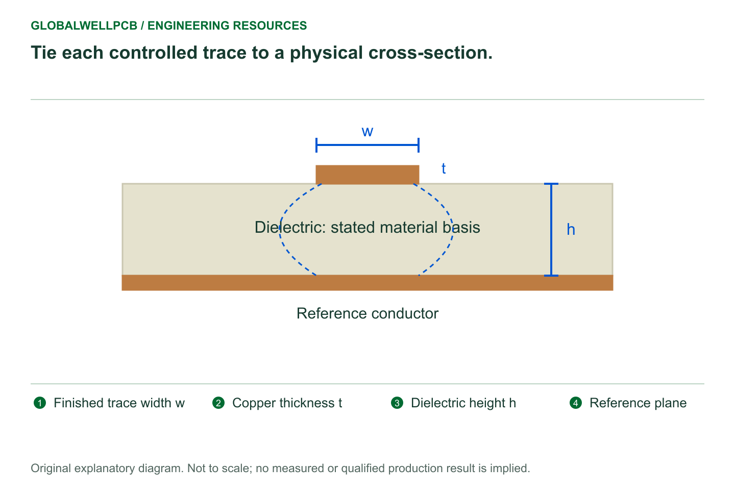
Separate nominal design inputs from offered manufacturing construction and acceptance requirements. The fabricator’s proposed dielectric thickness may be a processing target, while the design model needs a corresponding finished structure. Ask what the quoted number represents and which variation is relevant to the electrical review.
KiCad’s stackup setup separately represents copper and dielectric physical parameters, and its documentation notes that stackup thickness influences via-length calculations and exported mechanical models. A consistent CAD stackup is therefore useful beyond the drawing itself. KiCad PCB Editor: configuring board stackup and physical parameters
Do not confuse a populated CAD dialog with a supplier-approved build. Keep the accepted construction revision visible in both the project record and the released fabrication documentation.
Use a stackup agreement table
The proposed table below links the construction decision to the person or evidence needed to close it. Adapt the roles to the actual project.
| Decision | Design input | Fabrication response | Closure evidence |
|---|---|---|---|
| Overall build | Finished thickness and mechanical interfaces | Proposed construction and thickness interpretation | Accepted stackup revision and mechanical drawing |
| Layer function | Signal, plane, and reference assignments | Layer sequence and fabrication naming | Matching layout layer map |
| Dielectrics | Exact material needs and electrical model conditions | Core and bond-layer construction | Traceable material and construction record |
| Copper | Starting or finished copper by layer | Offered copper definition and process assumptions | Agreed drawing notes |
| Interconnect | Required layer-to-layer paths and pad geometry | Feasible via spans and process sequence | Accepted via table or cross-section |
| Verification | Electrical and mechanical questions to resolve | Proposed coupons, measurements, and records | Agreed acceptance and reporting plan |
An open row is not automatically a reason to stop all layout work. It is a reason to identify what can proceed without creating rework and what must wait for agreement.
Check vias against the proposed build
Map each via family to its start and stop layers. Identify which connections must reach a surface and which can remain internal. Ask the fabricator to explain the proposed process sequence, including any sequential build steps, rather than assuming that a via symbol implies a particular manufacturing route.
Review the interface between via structure and component lands. If a pad must also serve as an assembly surface, the via treatment is part of the stackup discussion. If a signal transition leaves an unused conductive section, decide whether its electrical effect needs analysis. Neither issue is answered by reducing the nominal hole diameter alone.
Distinguish an approved interconnect concept from approval of the complete board. A process demonstrated on another stackup may not cover the same materials, layer spans, pad interfaces, or thermal history. Request evidence relevant to the proposed construction and intended operating conditions.
Resolve material substitutions as design changes
A material-family label is useful for discussion but often too broad for release. Capture the exact proposed grade, construction, and relevant supplier documentation. If the supplier proposes an alternative, compare the properties that drive this design rather than accepting a single matching headline number.
For example, an electrical model may depend on a dielectric value under stated conditions, while assembly and reliability review may depend on other thermal and mechanical properties. One apparently similar property does not settle every question. Define which changes require electrical reanalysis, mechanical review, or qualification before approving the substitute.
This is also the point to resolve symmetry and copper-distribution concerns with the fabricator. Ask for a build-specific assessment rather than a guarantee based only on a visually symmetric layer sketch. The stackup drawing describes part of the structure; the actual copper artwork and process sequence supply additional context.
Freeze an agreement and control what happens next
Before final routing, issue the accepted stackup with a revision and link it to the project. Update the CAD model, routing rules, impedance calculations, and via definitions from that same agreement. Review any remaining departures explicitly.
If a later manufacturing proposal changes a dielectric thickness or material, assess the affected structures before accepting it. The important question is not whether the revised board still has the same number of layers. It is whether the construction remains suitable for the electrical, mechanical, and process decisions already made.
At fabrication release, compare the exported layer order and drawing against the accepted stackup. At first-build review, connect the supplied construction and measurement records to that revision. This closes the loop between the intended build, the purchased build, and the evidence available for the next order.
References and method
This article uses AI-assisted drafting and document review of the specified TI reference-plane and stackup sections and KiCad’s physical-stackup guidance. The agreement table is an original coordination tool. No actual stackup, supplier process, EMC result, or reliability test was approved during this review.