GlobalWellPCBPCB & PCBA Manufacturing
PCB Fabrication

HDI & Microvia Capabilities

Define HDI by the connections your design requires: which layers each via joins, how the dielectric is built and how the pad will be finished. A layer-by-layer via map is more useful for review than an unsupported HDI order label.

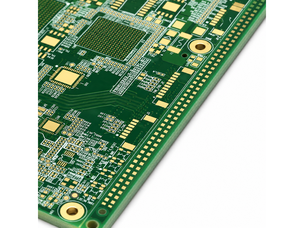
Close-up of high-density PCB traces and BGA pad array
PCB trace and BGA pad detail. Illustrative example; layer count and via structure are reviewed separately.
Capability register

Scope and conditions

Read each value together with its board type and review conditions.

0.075mmLaser drilling reference
Rigid and rigid-flex entries; depth review
1:1Laser aspect ratio
Rigid and rigid-flex entries
8LAny-layer example
One documented project, not an HDI maximum

Published limits apply to their stated board type. Layer count, copper weight and minimum geometry require a combined engineering review.

Capability register

Microvia and buried-connection register

Drilling figures belong to the stated board type. They do not establish a maximum HDI order or approve a complete stackup.

On smaller screens, scroll within the table to see every column.

ParameterPublished capabilityApplies toReview conditions
Minimum laser drill0.075mmRigid and rigid-flex published entriesDielectric depth, layer span, capture pad and final hole definition
Laser aspect ratio1:1Rigid and rigid-flex published entriesAgree processed depth and diameter; separate from mechanical-hole aspect ratio
Flex laser drill0.1mmFlex published entryProtective construction, dielectric and layer span
Blind and buried structuresListed product typeRigid published product entrySupply every start/end layer and the corresponding stackup
Filled, capped or stacked featuresConstruction reviewed from filesProject-defined via structureSpecify fill, cap, plating, stacking and inspection requirements; no universal combination is implied
Engineering review

A via map defines the build

Give every via family a distinct name and unambiguous layer span.

Connectivity
Identify start and end layers, plated status, drill or finished diameter and the electrical role. Separate mechanical through holes from laser features.
Pad and protection
Show capture and target pads, pad openings, solder-mask relationship and whether a via is exposed, covered, filled or capped.
Build sequence
Provide the proposed dielectric construction and any sequential lamination requirements. Allow engineering to review the sequence against the actual material and feature set.
Documented project examples

Documented any-layer and sequential-build examples

These examples describe individual structures in our project reference material. They do not establish a general maximum or guarantee the same combination for a new design.

8L any-layer HDI

The reference records 8L any-layer HDI with RO4450F + HTG hybrid pressing, 4.5mil inner hole-to-line and a chip-testing-board description. This documents one construction; it does not establish maximum HDI order.

Individual engineering example; the combination is reviewed for each project.

20L blind-via structure

A separate example records 20L, three pressing cycles, blind connections 1–4 / 17–20L and 3/3mil geometry. The pressing count is a feature of this example.

Individual engineering example; the combination is reviewed for each project.

Engineering review

Specify filling and acceptance together

A via in a component pad needs a more complete instruction than its hole diameter.

Identify which pads contain vias and state the required fill and finished surface. If the drawing requires a cap or stacked structure, show it explicitly so that fabrication, assembly and inspection can review the same requirement.

Define the evidence needed for acceptance, such as the agreed cross-section locations and criteria for the selected construction. Do not use a bare-board inspection statement as a substitute for an assembled-joint inspection plan.

Engineering review

HDI RFQ checklist

Submit a construction that can be reviewed without guessing the connections.

Core files
Fabrication layers, full drill data, via map, stackup, material identity, finished copper and controlled geometry.
Assembly interface
Component package and land-pattern data for fine-pitch escape areas; flag via-in-pad and any planarity-sensitive pads.
Decision points
Identify essential layer spans, any allowed routing or pad changes, impedance requirements and the requested verification records.
RFQ checklist

Send the files that define your build

Include the drawing revision and acceptance requirements. The engineering review confirms the manufacturable combination before quotation.

PCB fabrication

  • Gerber or ODB++ fabrication data and the board outline
  • Layer stackup, material identity, finished copper and board thickness
  • Drill data, impedance targets, surface finish and inspection requirements
Request PCB quote

PCB assembly

  • PCB fabrication package and an itemized BOM with manufacturer part numbers
  • CPL / pick-and-place data, assembly drawings and component polarity
  • Component sourcing scope, programming files and the agreed test procedure
Request PCBA quote
Engineering FAQ

Questions before you quote

What is the maximum supported HDI order?

A universal maximum HDI order is not established in the published capability data. Send the stackup, via spans, pad structure and package geometry for a construction-specific review.

Does the 8L any-layer example approve every any-layer design?

No. It documents one reference structure. Material, dielectric depth, via geometry, filling, stacking and acceptance criteria must be reviewed for each design.

Can the mechanical aspect ratio be used for a laser microvia?

No. The capability table provides separate mechanical and laser entries. Use the processed depth and diameter for the actual hole family.

What should I include for via-in-pad?

Identify the affected pads, via size and layer span, required fill/cap, finished surface and the inspection criteria needed by the assembly.

Scroll to Top