High Current PCB
Plan the entire power path.
Not just the copper weight.
Prepare your high-current PCB project for fabrication review: define the load, copper construction, connections and thermal limits before locking the manufacturing specification.
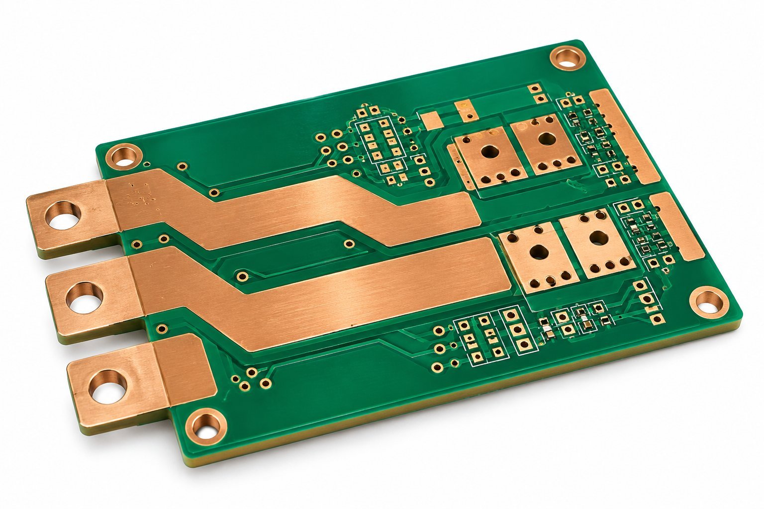
What is a high current PCB?
For related construction choices, review heavy-copper PCB, copper-base PCB, PCB assembly, functional-test planning.
A high current PCB is a board whose power paths must carry the specified load while keeping voltage loss and temperature within the project’s limits.
IPC-2152 relates conductor sizing to current and acceptable temperature rise. It is not a universal amperage label for an entire board or copper weight.
For an RFQ, identify the complete source-to-load route and its return path. Mark the connection points and specify the operating conditions that the proposed construction must satisfy.
- High current
- An electrical and thermal design requirement—not a particular layer count.
- Heavy copper
- A conductor construction choice that can support that requirement. “Heavy” and “thick” copper terminology varies between suppliers.
- High voltage
- A separate insulation question. Review working voltage and insulation requirements in addition to current, not in place of it.
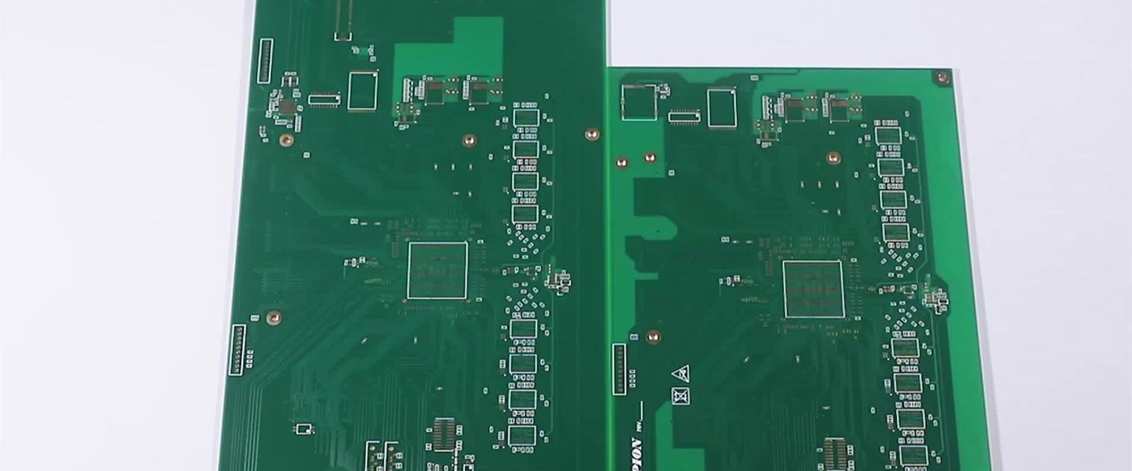
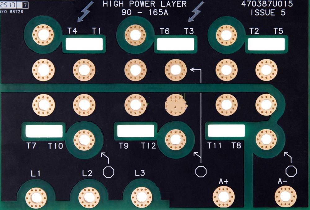
Choose the current path before
choosing the copper specification.
Compare practical design routes against the same electrical, mechanical and manufacturing requirements.
Wide pours and short routes
Increasing conductor cross-section or reducing length lowers resistance for the same material and temperature. Trace restrictions around pads and keepouts still belong in the review.
Ask in the RFQ: Which conductor dimensions must be maintained after fabrication?
Connected power layers
Via arrays can create low-impedance links between power layers. Placement matters: inspect the entry, transition and exit rather than simply adding more holes.
Ask in the RFQ: Which layers share each current path, and how are they connected?
Heavier or localized copper
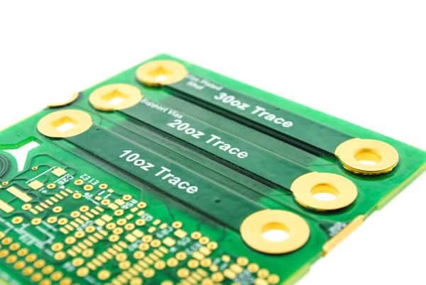
Heavier copper is one option. Local copper inlays or separate reinforcement are other engineering directions, but introduce additional construction or joining decisions.
Ask in the RFQ: Is the proposed construction manufacturable for this exact layout?
Options for Your Design. Send the proposed copper structure, dimensions and critical features to confirm manufacturing options for your high-current PCB.
Look for the limiting point
in the whole circuit.
Use this checklist to brief the designer, fabricator and assembly team on the same critical features.
Load profile and voltage-drop budget
Record sustained current, peak duration and repetition. Name the source and load measurement points, and state whether the resistance budget includes both the supply and return.
Finished copper, not an ambiguous label
Distinguish starting foil from the finished conductor. Outer-layer processing includes copper deposition; the foil label and the final copper requirement are not interchangeable.
Vias, terminals and narrow connections
Mark neck-downs, thermal-relief spokes, hole barrels and terminal lands. Specify power connections against the actual connector footprint and assembly requirements.
Heat removal and hot-spot limits
Document ambient conditions and the cooling arrangement. Continuous copper and appropriately connected thermal vias help move device heat into the board.
Switching loops and quiet sensing
Short, compact high-di/dt loops reduce parasitic inductance. Keep the current-sense pickup deliberate; Kelvin routing separates the measurement path from unwanted power-path voltage drops.
Small resistance.
Meaningful power loss.
For constant DC, estimate voltage drop and resistive heating from a known or assumed path resistance.
Not an ampacity calculator. This check does not size traces or vias, predict temperature, or verify IPC-2152 compliance. It assumes the entered resistance stays constant; it excludes switching loss and thermal feedback.
Turn the load requirement
into a clear fabrication brief.
Use the table as an RFQ input checklist—not as a list of guaranteed manufacturing limits.
| REVIEW ITEM | INFORMATION TO PROVIDE | CONFIRMATION BASIS |
|---|---|---|
| Electrical duty | Continuous current by net; peak current, pulse duration, repetition and fault-clearing assumptions. | Annotated current-path map and operating-mode table. |
| Voltage-drop budget | Maximum acceptable drop between clearly identified source and load measurement points. | State whether the return conductor and contacts are included. |
| Layer stackup and copper | Layer functions; base foil and required finished copper; minimum thickness and tolerance where critical. | Approved layer drawing, not a single copper-weight label. |
| Power-path geometry | Board outline; shortest allowed routes; narrow sections; keepouts and connector access. | Fabrication files plus marked critical conductor dimensions. |
| Vias and plated connections | Finished hole dimensions, plating requirements, land geometry and layer connections. | Drill table, padstack details and connector supplier requirements. |
| Material and thermal limits | Laminate grade, assembly exposure, ambient range, cooling and allowed hot-spot temperature. | Separate material requirements from the system thermal budget. |
| Connections and insulation | Terminal or press-fit details, soldering constraints, working voltage and insulation requirements. | Component drawings and the applicable product requirements. |
| Inspection and acceptance | Required records, sample plan, dimensional checks and any powered validation. | Written scope, acceptance limits and responsibility for each test. |
On smaller screens, scroll the table horizontally. Final values and tolerances belong in the approved project documentation.
Resolve the critical details
before production.
A suggested review sequence for a high-current project. Confirm the supplier’s scope and the customer’s validation responsibilities at quotation.
Define the duty
Share the current-path map, operating modes, thermal environment, quantity and drawing revision.
Agree the construction
Review copper distribution, etched features, hole requirements and assembly constraints. Document approved deviations.
Validate the prototype
Evaluate the populated design under agreed operating conditions. Record the critical drop and temperature measurements.
Control the release
Lock the fabrication revision, inspection records and acceptance criteria. Reassess relevant design changes.
A connected circuit is not
a qualified power path.
Separate bare-board acceptance from application-level load validation. Set the test scope before the build.
- Board-level inspection
- Request the agreed continuity, isolation, dimensional and workmanship checks. Specify additional copper or hole-plating evidence where needed.
- Powered prototype measurements
- Define assembly state, load profile, ambient conditions, cooling, measurement locations and stabilization criteria. Compare the measurements with the project’s stated limits.
- Records and change control
- Record the tested revision and configuration. Review relevant copper, terminal, material, cooling or operating changes before relying on an earlier result.
Bench testing remains important even after calculation and simulation. The Analog Devices reference illustrates this in a high-current Hot Swap design.
Thermal images and test reports should identify the tested board configuration, loading conditions and measurement method.
Illustrative review format — not a customer project: Board revision and copper construction | Load and duty cycle | Ambient and cooling conditions | Measurement method and locations | Agreed temperature limits | Recorded measurements | Review decision. This is a blank test-record outline, not a thermal test result.
Different loads.
Different review priorities.
Suggested briefing topics for four application types—not GlobalWellPCB customer case studies.
Power conversion
Provide rail currents, switching conditions, loss budgets and the available cooling arrangement.
Motor control
Include operating, starting and stall scenarios, together with the power-stage and sensing requirements.
Battery systems
Distinguish monitoring-only circuits from charge, discharge and protection power paths.
Power distribution
Identify each branch load, terminal connection, return path and voltage-drop measurement point.
High Current
PCB FAQs
Practical questions to resolve before requesting a quote.
Is a high current PCB the same as a heavy copper PCB?
No. High current is the electrical requirement; heavy copper describes the conductor construction. A project may use wide pours, multiple connected layers, heavier copper or a separately reviewed reinforced path. The choice still needs an electrical and thermal assessment.
How much current can a 2 oz PCB carry?
Copper weight alone is not enough to assign a current rating. Specify the conductor width, finished thickness, route length, layer position, allowable temperature rise and cooling conditions. Also check the interconnections on that route.
How many vias should a high-current connection use?
There is no universal amps-per-via rule for every stackup. Review barrel plating, hole geometry, connection length, via placement and the copper around the array. TI recommends multiple vias near relevant current entry and exit locations in its motor-driver layout guidance.
Does a metal-core PCB automatically solve high-current routing?
No. In an insulated-metal-substrate construction, the metal carrier is separated from the circuit copper by a dielectric. A heat-spreading substrate is not automatically the electrical conductor for the load current.
What is the difference between continuous, peak and fault current?
Continuous current describes sustained operation. Peak current also needs a duration and repetition rate. Fault current needs a protection and clearing-time definition. Include these separately in the RFQ; a continuous-current discussion should not be read as approval of every transient condition.
Will an ordinary bare-board electrical test prove the current rating?
Do not treat a continuity and isolation check as a powered-load qualification. Define a separate prototype test plan with the actual assembly, current profile, cooling arrangement, voltage-drop limit and temperature measurement points. Agree who performs the tests and what records are required.
What should I include for a technical quotation?
Prepare the fabrication data, drill files, stackup, board drawing, quantity and revision. Add an annotated current-path map, continuous and peak requirements, copper and plating requirements, thermal conditions, connector details and the requested inspection records.
What affects the cost of a high current PCB?
Use the quote to compare copper construction, geometry, holes, material selection, panel utilization and the requested verification work. Thicker copper can change the manufacturable feature set; do not compare nominal copper weight without comparing the rest of the fabrication package.
Related PCB technologies
Technical references and scope
Manufacturer references below support the engineering discussion. Their products, figures and capabilities are not GlobalWellPCB production claims. IPC reference [1] is a public scope-and-contents excerpt, not the full standard.
- [1]IPC · IPC-2152 scope and contents (public excerpt, PDF)
- [2]Würth Elektronik ICS · PCB construction and high-current contact considerations
- [3]Texas Instruments · Best Practices for Board Layout of Motor Drivers, Rev. B (PDF)
- [4]Analog Devices · Pad layout and Kelvin sensing for low-value shunts
- [5]Analog Devices · LTC4218 high-current design: sharing, sensing and validation
- [6]Würth Elektronik · BASIC PCB design: foil, plating and copper distribution
- [7]Texas Instruments · Optimizing Layout for Synchronous Buck Converters
Use the references below when planning your high-current PCB. Include the applicable standards, finished construction and acceptance requirements with your enquiry.