PCB Impedance
Control
Bring your stackup, trace geometry and verification requirements together for a better-defined controlled-impedance PCB build.
What is PCB impedance control?
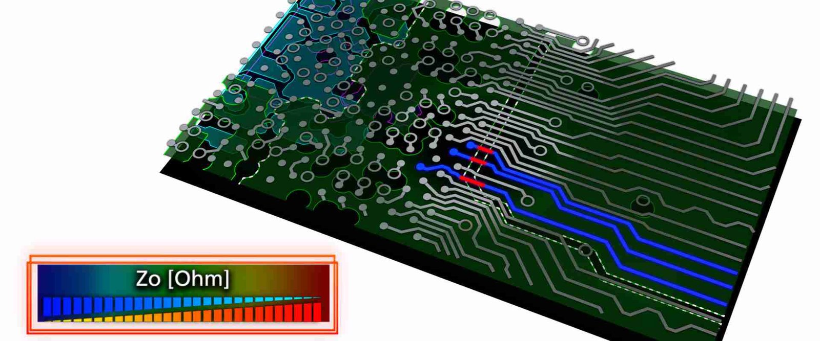
PCB impedance control is the design and fabrication of transmission lines to meet a specified characteristic impedance within an agreed tolerance. It connects the electrical target to the material, conductor geometry and reference-plane arrangement of the finished board.
When signal transitions are fast compared with the time needed to travel along an interconnect, the route must be treated as a transmission line. Edge rate and electrical length matter—not just the clock frequency printed on a schematic.
Identify the nets that need control, then agree how the construction and measurements will support those requirements. A single impedance note without layer or structure information leaves important questions unresolved.
Same target.
Different physical structures.
The signal layer alone is not enough. Define the surrounding dielectric and conductors used in the impedance model.
Surface Microstrip
An outer-layer trace above a reference plane. Air and dielectric influence the fields; a solder-mask coating changes the structure and should be included where applicable.
Specify: width, height, finished copper and mask.
Stripline
An internal trace between reference planes. The two dielectric separations need not be equal: symmetric and offset striplines require the appropriate model.
Specify: both reference planes and dielectric heights.
Differential Pair
Two coupled traces, shown here as edge-coupled microstrip. Pair spacing is part of the impedance geometry, not simply a routing clearance.
Specify: pair width, edge-to-edge gap and symmetry.
Schematic cross-sections, not to scale. W = trace width; S = pair gap; H = dielectric height. Solder mask is omitted from these drawings for clarity. Coplanar and other constructions require their own models.
Control the construction.
Not just the trace width.
Review these variables together. A dimension that works in one stackup is not a universal solution for another.
Finished trace width
For a fixed microstrip construction, a wider conductor generally lowers characteristic impedance. Use the fabricated conductor profile, not only the nominal artwork width.
Dielectric separation
Increasing the trace-to-plane distance generally raises microstrip impedance when other parameters stay fixed. For stripline, include the separation to both planes.
Differential pair gap
Coupling changes as pair spacing changes. For a typical edge-coupled pair with the rest of the structure fixed, increasing the gap generally raises differential impedance.
Dielectric properties
Use a dielectric constant appropriate to the material, construction and modeling conditions. Treat a laminate substitution as an electrical design change, not just a purchasing change.
Copper profile & processing
Finished thickness, plating and etch shape affect the model. A trapezoidal trace has different top and bottom widths; extra calculator decimal places do not remove fabrication variation.
Solder mask & nearby copper
Outer-layer coating and adjacent copper can change the electromagnetic environment. State mask coverage and copper clearances rather than assuming the bare-microstrip model applies.
Turn an impedance value
into an actionable requirement.
For each controlled structure, identify the net group, layer, reference plane, target and acceptance tolerance.
Scroll horizontally to view all columns.
| Example net group | Mode / target | Layer / reference | Tolerance | Geometry & verification |
|---|---|---|---|---|
| RF signal path | Single-ended / 50 Ω | L1 / L2 reference | State the design requirement | Review finished width, dielectric height, mask and coupon. |
| Differential group A | Differential / 90 Ω | L1 / L2 reference | Use the applicable interface specification | Review pair width, gap, reference continuity and measurement mode. |
| Differential group B | Differential / 100 Ω | L3 / L2 + L4 references | Confirm before fabrication | Review both dielectric heights, pair geometry and coupon mapping. |
The values above are examples, not universal settings for a protocol. For example, TI’s TUSB564-Q1 layout guidance specifies 90 Ω differential with ±15% tolerance; use the guidance for your actual device and interface.
Separate the target from the acceptance plan.
State whether dimensions are fixed or may be adjusted with approval. Identify the governing file revision, coupon-to-net mapping and the required report. Resolve conflicts between drawing notes and the impedance table before release.
Do not assume that ±10%, ±5% or another tolerance is included automatically. Ask for feasibility, test scope, pricing and lead time to be confirmed against the complete construction.
Prepare the requirements for reviewImpedance tolerance range
Translate a nominal target and percentage into limits.
Limits = target × (1 ± tolerance / 100). This is arithmetic only—not a trace-width solver, measured result or manufacturing commitment.
A clear path from design intent
to manufacturing release.
Bring the open questions forward, before they become production changes.
- 01
Share the complete inputs
Send fabrication data, the controlled-net table, stackup assumptions and quantity. Identify fixed dimensions, permitted changes and the required evidence.
- 02
Review the construction
Resolve material selection, finished dielectric heights, copper geometry and reference layers. Agree which structures and tolerances require confirmation.
- 03
Approve before release
Approve the file revision, proposed geometry changes and acceptance plan. Include coupon design, measurement mode and reporting in the agreed build scope.
- 04
Build to the agreed scope
Carry out the approved fabrication and verification plan. Review the agreed records, handle deviations explicitly and retain the final configuration for repeat orders.
Need fabrication and assembly together? Explore the PCB and PCBA project scope.
Define what the test proves.
The test name is only the beginning. Agree the structure, measurement method and acceptance rules.
Representative coupon construction
A coupon is a separate test structure fabricated with the production panel. Its layer, conductor geometry, dielectric and coating should represent the controlled structures being checked. A coupon result is not a direct measurement of every routed net.
Time-domain reflectometry
TDR applies a fast transition and observes reflections to characterize impedance along a structure. The setup, launch and resolution influence the response; agree how the useful measurement region will be evaluated.
Report and acceptance requirements
Request the board revision, panel/coupon identity, structure, target, limits, measured result and relevant setup conditions. Define sampling, traceability and the handling of out-of-limit results in the order requirements.
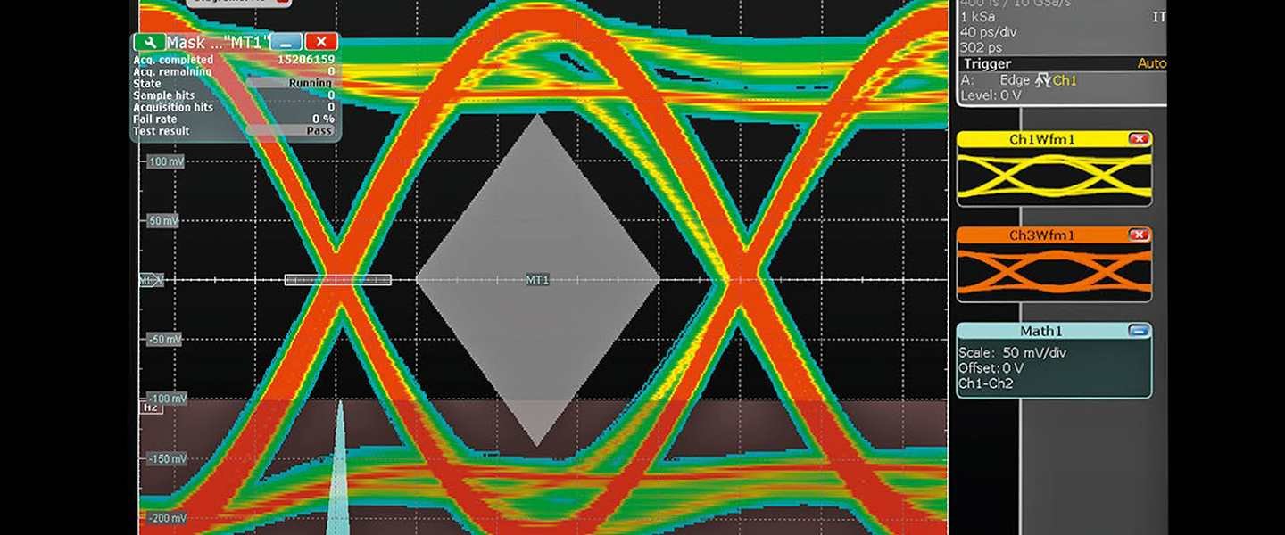
An impedance result alone does not certify insertion loss, eye opening or interface compliance. Specify separate channel or frequency-domain verification where required. TDR availability, coupons, sampling and supplied reports must be confirmed in the quotation.
PCB Impedance
Control FAQs
Practical answers before you finalize the layout or request a quotation.
What is the difference between controlled impedance and impedance matching?
Controlled impedance describes the specified transmission-line construction and its allowed variation. Matching concerns how that line interacts with the source, load and transitions. A board can meet its trace-impedance requirement while a connector or termination still introduces mismatch.
What trace width gives 50 Ω on a PCB?
There is no universal width. The answer depends on the line structure, finished dielectric height, material properties, copper profile and any coating. Establish the stackup first, then solve and approve the geometry. A width copied from a different board may not produce the same impedance.
Is a 100 Ω differential pair simply two 50 Ω traces?
Not necessarily. Coupling between the traces changes their behavior. For a symmetric balanced pair, differential impedance is twice the odd-mode impedance. The impedance of each isolated trace is a different quantity, so specify and model the pair as a coupled structure.
Can an FR-4 PCB have controlled impedance?
Yes. Controlled impedance is a property of the specified transmission-line construction, not a synonym for an RF laminate. Material loss and the complete channel requirements still need separate review; achieving an impedance target does not demonstrate a loss budget.
Should I specify ±10% or ±5% impedance tolerance?
Use the tolerance required by your design and acceptance specification, then request a feasibility review. Neither value should be treated as an automatic capability promise. Confirm the full stackup, measurement approach, cost and delivery implications before committing to the order.
Does coupon testing measure every signal trace?
No. A representative coupon checks a test structure fabricated alongside the boards. Product-specific transitions, branching and other local geometry are not all reproduced by that coupon. Agree the coupon mapping and any additional product-level verification you need.
Does the standard bare-board electrical test verify impedance?
A continuity/isolation test and a transmission-line impedance measurement address different requirements. Specify TDR or another agreed impedance method separately. Likewise, an impedance report is not by itself an insertion-loss or full interface-compliance report.
What files are needed for a controlled-impedance PCB quote?
Provide fabrication data, drill files, board dimensions, quantity, the proposed stackup and a controlled-net table. Include targets, tolerances, reference layers, fixed dimensions, allowed adjustments and required reports. Add BOM and placement files when assembly is part of the project.
Technical references
- [1] Polar Instruments — Controlled impedance fundamentals
- [2] Polar Instruments — Impedance and signal-integrity glossary
- [3] Polar Instruments — Microstrip structures
- [4] Polar Instruments — Stripline structures
- [5] Polar Instruments — Field-solver precision and real fabrication geometry
- [6] Polar Instruments — Controlled-impedance test coupons
- [7] Texas Instruments — TUSB564-Q1 application and layout guidance
- [8] Keysight — TDR/TDT Concepts
- [9] Analog Devices — TDR and high-frequency verification
- [10] Analog Devices — Interfacing high-speed signals
- [11] Polar Instruments — Transmission-line configurations
Use these impedance-design references when preparing your stackup and controlled-net table. Your quotation confirms the manufacturing and testing requirements for your board.