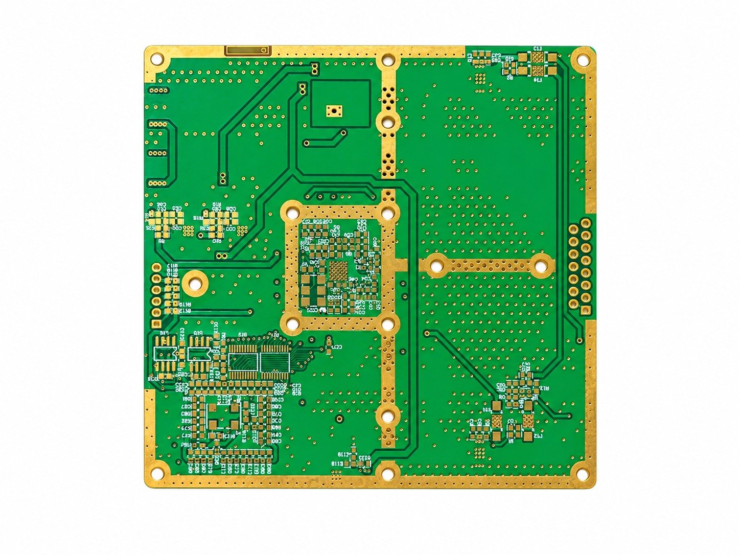
Rogers4835 + Isola370HR
A 6L reference records this hybrid material combination with blind vias. A new design still needs exact grade and bonding-layer approval.
Individual engineering example; the combination is reviewed for each project.
An RF or high-speed board starts with a controlled construction. Identify the laminate and bonding materials, copper, dielectric thickness and reference layers, then define impedance and via-transition requirements for the signals that matter.
Read each value together with its board type and review conditions.
Published limits apply to their stated board type. Layer count, copper weight and minimum geometry require a combined engineering review.
The material examples below establish prior project combinations. No general material-stock, frequency or loss specification is inferred.
On smaller screens, scroll within the table to see every column.
| Parameter | Published capability | Applies to | Review conditions |
|---|---|---|---|
| Laminate and bonding identity | Exact manufacturer and grade | Every core and bond layer | State product revision, thickness and any permitted equivalent |
| Copper construction | Defined per layer | Signal, reference and plating layers | Finished copper and any foil-related requirements belong in the stackup |
| Single-ended tolerance | ±5Ω at targets ≤50Ω; ±7% at targets >50Ω | Rigid published impedance entry | Target, layer, reference, geometry and agreed test method |
| Differential tolerance | ±5Ω at targets ≤50Ω; ±7% at targets >50Ω | Rigid published impedance entry | Pair geometry, layer transitions and agreed coupon |
| Backdrill and blind spans | Defined by via map | Project-specific transitions | Start/end layers, diameter, residual-stub requirement and keepout |
| Material properties for design | Use the specified material documentation | Electrical and thermal design | Define the test condition for any requested Dk, Df or thermal value |
These examples describe individual structures in our project reference material. They do not establish a general maximum or guarantee the same combination for a new design.
A 6L reference records this hybrid material combination with blind vias. A new design still needs exact grade and bonding-layer approval.
Individual engineering example; the combination is reviewed for each project.
A 12L reference records these materials and 3.0mm board thickness. Those values belong to the example.
Individual engineering example; the combination is reviewed for each project.
A 14L reference records RO4003C + HTG, blind spans 1–10 / 11–14L and backdrill entries 1–4 / 1–9L.
Individual engineering example; the combination is reviewed for each project.
An 8L reference records this hybrid combination, blind spans 1–4L / 8–5L and a plated gold edge.
Individual engineering example; the combination is reviewed for each project.
A target impedance alone leaves several construction decisions open.
Impedance evidence and application performance are different acceptance requirements.
Specify impedance targets, tolerance, coupon structure, measurement reporting and the link between the coupon and product stackup. Where product-level RF or signal testing is required, provide the method, fixture/interface and pass criteria.
Name the properties used in your design model with their material and test conditions. A material family name or an example board does not supply a universal electrical performance value.
Make the material and controlled interfaces easy to identify.
Send fabrication data, drill files, exact stackup and material schedule, copper requirements, impedance table and via/backdrill map. Flag edge contacts, connector launches, cavities or other critical mechanical interfaces in the drawing.
List approved substitutions or state that material changes require written approval. Include the requested verification records and any application-level test specification with the initial RFQ.
Include the drawing revision and acceptance requirements. The engineering review confirms the manufacturable combination before quotation.
The named materials come from documented project examples. Material identity, availability and the construction for a new order are confirmed during quotation.
The published data does not establish one. Provide the signal requirement, material construction and the requested test conditions for project review.
Supply the proposed exact grade and relevant documentation. Review electrical, thickness and processing requirements and obtain approval before changing the construction.
An impedance result addresses the agreed impedance requirement. Product-level RF performance needs its own defined test setup, interfaces and acceptance criteria.