GlobalWellPCBPCB & PCBA Manufacturing
PCB Fabrication

Flex PCB Capabilities

A flex circuit must fit its electrical route and its installed shape. Review the flexible stackup, copper, protective layers, stiffeners and bend zones together, and identify whether the circuit is formed once or moves in service.

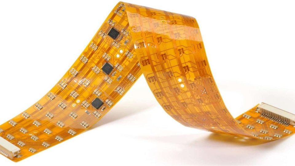
Amber flexible circuit folded into a bend with visible traces and components
Bent flexible circuit. Illustrative example.
Capability register

Scope and conditions

Read each value together with its board type and review conditions.

8LMaximum layers
Flexible PCB construction
0.1–0.5mmBoard thickness
Published flex range; local stiffeners separate
2ozInner / outer copper
Flex limits; each layer reviewed

Published limits apply to their stated board type. Layer count, copper weight and minimum geometry require a combined engineering review.

Capability register

Flex construction register

These values apply to flex PCB and do not inherit the rigid-board copper or layer limits.

On smaller screens, scroll within the table to see every column.

ParameterPublished capabilityApplies toReview conditions
Maximum layers8LFlex constructionLayer arrangement and intended bending behavior
Board thickness0.1–0.5mmFlexible constructionDefine the flex thickness separately from stiffened locations
Inner / outer finished copper2oz / 2ozFlex copper layersCopper type, geometry and bend zone
Inner trace / space3/3milInner flex patternCopper thickness and local density
Outer trace / space3.5/4milOuter flex patternCopper, protective layer and pad openings
Mechanical / laser drilling0.1mm / 0.1mmRespective flex drilling processesHole type, processed depth and layer span
Mechanical aspect ratio10:1Flex mechanical drillingConfirm actual diameter and processed thickness
Capability register

Outline, protection and markings

Show the finished circuit outline and all stiffened regions on the same controlled drawing.

On smaller screens, scroll within the table to see every column.

ParameterPublished capabilityApplies toReview conditions
Process panel500 × 1200mmFlex process panelManufacturing margins and material format
Finished board range5 × 10mm minimum; 9.8 × 19.8inch maximumIndividual flex outlineHandling, panelization and protection
Contour tolerance±0.05mmFlex outlineDatum scheme and critical connector features
Protection entriesGreen solder mask; black, yellow and white PIOptions listed for flexConfirm protective construction, openings and adhesive details
Mask clearance / dam3mil / 8milFlex solder maskCheck the selected mask or PI construction separately
Legend width / height4mil / 23milFlex legendColor, protected area and readability
Capability register

Bend references need a defined duty

The sheet gives thickness-based design references. They are inputs to review, not a fatigue-life guarantee or an automatic approval for every stackup.

On smaller screens, scroll within the table to see every column.

ParameterPublished capabilityApplies toReview conditions
Single-sided reference radius3–6 × board thicknessFlex reference constructionCopper, protection, bend direction and installed geometry
Double-sided reference radius6–10 × board thicknessFlex reference constructionLayer arrangement and bend-zone features
Multilayer reference radius10–15 × board thicknessFlex multilayer referenceLayer count and any bonded/unbonded regions
Dynamic bending reference radius20–40 × board thicknessMotion in serviceRequired cycle life, stroke, speed and environment must be supplied
Strain fillet width1.5 ±0.5mmFlex transition detailConfirm the actual transition and drawing requirement
Engineering review

Define the flex zones and stiffeners

A flat fabrication file cannot fully communicate the installed circuit.

Installed shape
Supply bend locations, direction and required radius with an assembly or installation drawing. Mark areas that must stay flat.
Stiffener definition
Identify each stiffener material, thickness, adhesive, side and outline. Separate connector support dimensions from the flexible circuit thickness.
Assembly interface
Show component locations, connector mating surfaces, soldering areas and carrier or panel requirements. Keep assembly access visible in the review.
Documented project examples

An example outside the tabulated thickness range

These examples describe individual structures in our project reference material. They do not establish a general maximum or guarantee the same combination for a new design.

8-layer flexible reference

The project reference records 8-layer flex, 3/3.5mil, 0.8mm and green flex solder mask. The 0.8mm entry is specific to that recorded structure; it does not replace the general 0.1–0.5mm range or establish bend performance.

Individual engineering example; the combination is reviewed for each project.

Engineering review

Flex RFQ package

Describe the mechanical function as carefully as the net routing.

Send fabrication data, the flex stackup, copper requirements, finished outline, protective-layer openings and stiffener drawings. Include the installed shape and separate static forming from repeated motion.

For controlled impedance, supply the target, nets, reference layer and acceptance requirement. The flex table lists single-ended and differential tolerance as ±5Ω at targets ≤50Ω and ±10% above 50Ω; the agreed stackup and test method still need review.

RFQ checklist

Send the files that define your build

Include the drawing revision and acceptance requirements. The engineering review confirms the manufacturable combination before quotation.

PCB fabrication

  • Gerber or ODB++ fabrication data and the board outline
  • Layer stackup, material identity, finished copper and board thickness
  • Drill data, impedance targets, surface finish and inspection requirements
Request PCB quote

PCB assembly

  • PCB fabrication package and an itemized BOM with manufacturer part numbers
  • CPL / pick-and-place data, assembly drawings and component polarity
  • Component sourcing scope, programming files and the agreed test procedure
Request PCBA quote
Engineering FAQ

Questions before you quote

Can every 8-layer flex circuit bend dynamically?

Layer count alone does not define motion capability. Provide the flexible thickness, construction, bend radius and required motion duty for review.

Are stiffeners included in the published flex thickness range?

Specify the flexible construction and each local stiffener separately. A finished thickness at a connector cannot be assumed to describe the moving flex area.

Why does the reference example show 0.8mm?

That thickness belongs to the documented example. It is not a revision of the general 0.1–0.5mm flex range, and a similar construction needs individual review.

Which files are needed for a moving flex circuit?

Add the motion and installation drawing, bend radius, direction and required duty to the fabrication package, stackup and stiffener definition.

Scroll to Top