High Frequency
PCBs
RF and microwave PCB fabrication, with low-loss materials, controlled impedance and a stackup built around your signal requirements.
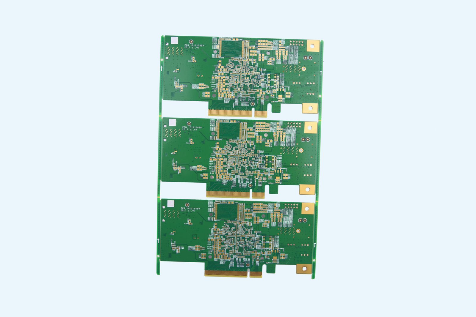
What are high frequency PCBs?
For related construction choices, review Rogers PCB materials, antenna PCB manufacturing, controlled-impedance requirements.
High frequency PCBs are printed circuit boards engineered to carry RF and microwave signals with controlled loss, impedance and phase behavior. Their performance depends on the dielectric material, copper structure, circuit geometry and complete signal path.
Compared with an ordinary FR-4 build, the specification needs to describe more than connectivity. It should identify which electrical characteristics matter, how they will be modeled and what evidence will be used to accept the finished board.
Start with the operating band, signal-path length and allowable loss. Then select the laminate and construction together. A material name alone is not a finished-board performance specification.
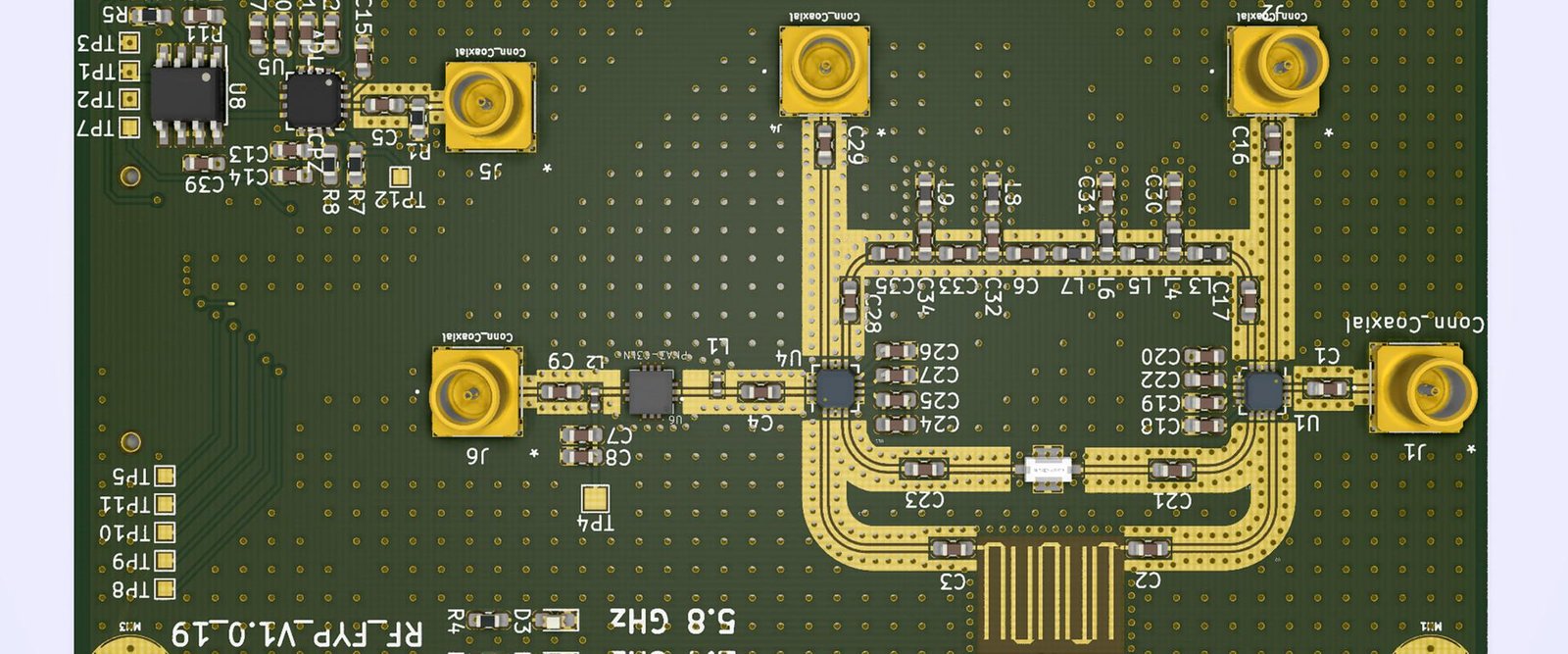
Choose a laminate around
your loss budget.
Compare electrical properties alongside fabrication, temperature stability, copper profile and the actual stackup.
Scroll horizontally to view all columns.
| Laminate | Process DkNominal ± tolerance | Design DkTypical | Df at 10 GHzTypical | Selection considerations |
|---|---|---|---|---|
| RO4003C™ Hydrocarbon / ceramic | 3.38 ± 0.05 | 3.55 | 0.0027 | Low-loss RF option with FR-4-like processing. Not UL 94 V-0 rated; check the product’s flame-rating requirement. |
| RO4350B™ Hydrocarbon / ceramic | 3.48 ± 0.05 | 3.66 | 0.0037 | UL 94 V-0-rated laminate for RF designs. Review the copper variant, dielectric thickness and circuit model. |
| RT/duroid® 5880 Glass-reinforced PTFE | 2.20 ± 0.02 | 2.20 | 0.0009 | Very low dielectric loss. Review the specific PTFE fabrication route, handling and mechanical requirements. |
Dk values above are published material-characterization/design values; confirm frequency, method and construction in the current manufacturer documentation. Df values are typical at 10 GHz. Do not interchange process and design Dk in a field solver. Grade, thickness, copper and availability require project confirmation.
Look beyond the lowest Df.
Copper roughness and line geometry also affect insertion loss. Temperature-dependent Dk and dimensional behavior matter when phase or resonance must remain stable.
Higher-Dk laminates may help reduce circuit size, while bonding materials must support the chosen multilayer construction. The best candidate is the one that meets the full design brief.
Include your preferred laminate in the RFQMake the stackup part
of the RF design.
For a hybrid RF/digital board, review a low-loss RF region alongside the other dielectric layers. The bonding system, thickness control and processing compatibility must be agreed as one construction—not selected independently.
- Choose the transmission-line structure
- State whether the design uses microstrip, grounded coplanar waveguide or stripline. Include the relevant dielectric thickness, copper geometry and reference conductors in the model.
- Protect the return path
- Keep the signal’s reference continuous and review layer transitions. Avoid routing critical paths across plane splits without a deliberate, verified return-path solution.
- Review transitions as part of the path
- Connector launches, vias and test fixtures can introduce local mismatch. Check their contribution rather than assuming a uniform trace model covers the entire route.
Specify what needs
to be controlled.
A useful high frequency PCB specification connects every critical feature to a clear review or acceptance requirement.
Scroll horizontally to view all columns.
| Review area | Include in your specification | Confirm during review |
|---|---|---|
| Operating requirements | Frequency band, path length, loss budget and relevant phase or environmental limits. | Which paths and operating conditions determine acceptance. |
| Laminate & bonding | Exact material grade, dielectric thickness, copper profile and permitted alternatives. | Availability, bonding compatibility and substitution approval. |
| Controlled impedance | Nominal impedance, tolerance, layer reference and line type for each controlled net. | Agreed geometry, coupon design and measurement/report scope. |
| Vias & registration | Drill data, RF transitions, critical layer alignment and any proposed stub treatment. | Feasibility of the requested combination, not isolated minimum features. |
| Surface finish & mask | Finish type, solder-mask openings and any controlled RF surface regions. | Compatibility with the circuit model, fabrication route and assembly process. |
| Inspection & RF evidence | Electrical test, dimensional checks, impedance or S-parameter results where required. | Ports or coupons, acceptance limits, test coverage and deliverable records. |
| Assembly & delivery | BOM, placement files, assembly drawings, quantity and requested delivery date. | Parts availability, assembly/test scope and confirmed schedule. |
Send your layer count, dimensions, tolerances and RF requirements with your board files. Your quotation will confirm the available processes, testing and delivery schedule.
A laminate upgrade does not fix a poor signal path.
Review the layout and the build together. A discontinuity at a launch, an interrupted reference plane or an unsuitable copper profile can undermine the intended benefit of a lower-loss dielectric.
Provide the controlled-net list and the design assumptions with the fabrication files so the engineering discussion starts from the same model.
Different systems.
Different RF priorities.
Use the application to frame the design review—not as a substitute for a complete electrical specification.
Wireless & Telecom
RF front ends, amplifier boards and antenna feed networks. Review dielectric loss, thermal behavior and repeatable transmission-line geometry.
Review focus: loss budget and matching
Radar & Industrial Sensing
Millimeter-wave sensing can make the laminate, copper profile and dimensional consistency especially important to the circuit design.
Review focus: geometry and material consistency
Antenna & Communications Systems
Feed structures and microwave paths may need predictable electrical behavior across environmental changes. Review the full material stability data.
Review focus: phase and environmental stability
Test & Measurement
RF evaluation paths and interconnect fixtures need well-defined ports and repeatable transitions so the measurement represents the intended structure.
Review focus: fixture and transition effects
Define the evidence.
Not just the test name.
Decide what must be demonstrated, at which ports or coupons, and against which limits before releasing the build.
Bare-board acceptance
List the required continuity/isolation checks and physical inspection records. Keep these separate from any RF performance acceptance requirements.
Impedance & discontinuities
Time-domain analysis can reveal local changes along an interconnect. Define the structure being measured and how the result will be assessed.
Frequency-domain performance
Specify insertion loss, return loss or other S-parameter limits across the required band. State the calibration, fixture handling and reporting expectations.
One contact.
A better-defined RF build.
Bring fabrication, component sourcing and assembly requirements into one coordinated project review.
Resolve the specification
Start with the material, stackup and controlled features. Make open questions and approval requirements visible before committing to production.
Review the checklistCoordinate the complete scope
Include sourcing and PCBA needs with your bare-board requirements. Identify approved part numbers and substitution restrictions at the outset.
Explore PCB & PCBA servicesAgree the release criteria
Confirm the file revision, build scope, inspection records and schedule before release. Keep technical and commercial decisions aligned.
View the quality approachHigh Frequency
PCB FAQs
Practical answers for material selection, design review and quotation.
What is a high frequency PCB?
A high frequency PCB is a printed circuit board designed so that its material, transmission lines, reference planes and transitions support the required RF or microwave performance. The important question is whether the finished signal path meets its loss, impedance and phase requirements, not whether the board carries a particular label.
When should I consider a low-loss material instead of FR-4?
Evaluate a low-loss laminate when the selected FR-4 construction cannot meet the loss budget, phase stability or impedance requirements over the required band. There is no universal cutoff frequency: trace length, geometry, copper roughness and the specific laminate all matter. Shorter or less demanding paths may still be suitable for FR-4.
Are Rogers RO4003C, RO4350B and RT/duroid 5880 interchangeable?
No. They differ in dielectric properties, resin systems and processing considerations. A change can require a new stackup, revised line geometry and fresh validation. RO4003C is not UL 94 V-0 rated; RO4350B is. Any material substitution should be explicitly approved rather than treated as a like-for-like replacement.
What is the difference between process Dk and design Dk?
Process Dk is associated with a specified material characterization method. Design Dk is a value supplied for circuit-design use under stated conditions. For example, Rogers lists RO4350B process Dk as 3.48 ± 0.05 and typical design Dk as 3.66. Confirm the appropriate model, frequency and construction before using either value.
Can RF laminates and FR-4 be combined in one PCB?
Hybrid construction is an option to review when RF and digital functions share a board. The bonding system, finished dielectric thickness, thermal behavior and fabrication sequence need to be compatible. Hybrid construction can change cost and complexity; it does not automatically preserve performance or guarantee a particular saving.
Does an impedance test verify insertion loss?
Not by itself. A time-domain impedance result helps identify mismatch along the path. Frequency-domain measurements are used to characterize insertion and return loss across the operating band. Agree the coupons or ports, calibration, fixture treatment and pass/fail limits before relying on a report for acceptance.
What do I need for a high frequency PCB quote?
Provide fabrication data, quantity, operating band, preferred laminate, stackup, copper specification, impedance targets, surface finish and any required measurement reports. Include the BOM and placement data for assembly. Material availability, achievable tolerances, test scope and delivery dates must be confirmed during project review.
Technical references
- [1] Rogers Corporation — RO4003C laminate properties
- [2] Rogers Corporation — RO4350B laminate properties
- [3] Rogers Corporation — RT/duroid 5880 laminate properties
- [4] AMD — PCB material properties and insertion losses
- [5] Texas Instruments — High-speed signal layout guidelines
- [6] Keysight — TDR/TDT Concepts
- [7] Rogers Corporation — SpeedWave 300P bonding material
- [8] Rogers Corporation — RT/duroid 6202 material stability
- [9] Rogers Corporation — RO4835IND LoPro radar laminates
- [10] Rogers Corporation — High-Dk RT/duroid laminates
Material values are references for selection, not guarantees of finished-circuit performance. Use the current manufacturer data and an approved project specification. Product names and trademarks belong to their respective owners.