HDI PCB Manufacturing and Microvia Design
HDI PCB manufacturing support for fine-pitch BGAs and compact electronics. Send your stackup, via structures and impedance requirements to confirm the construction for your design.
HDI requirements depend on component pitch, routing density, stackup, material, via structure and volume. Final specifications are confirmed during engineering review.
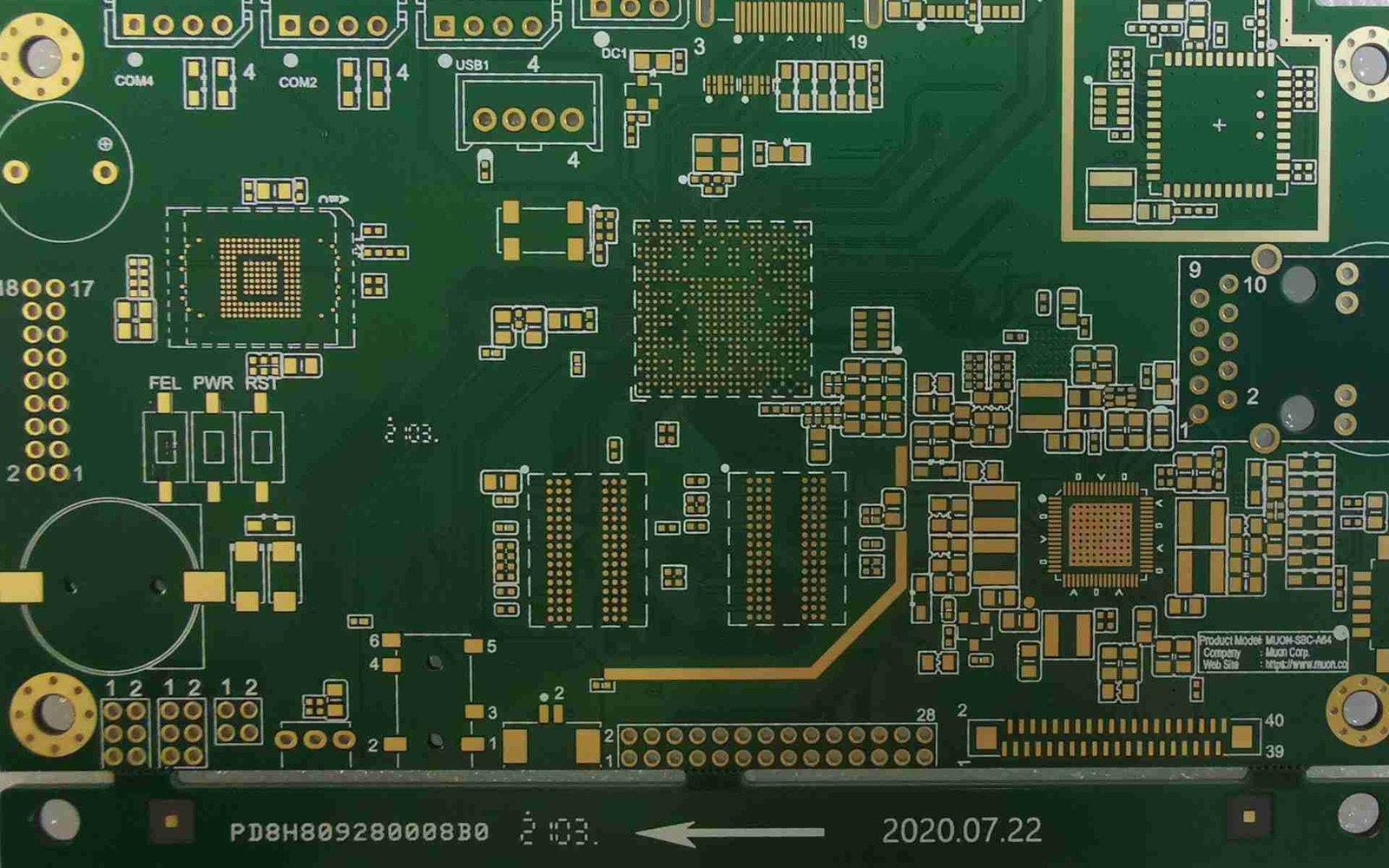
What is an HDI PCB?
An HDI PCB (High-Density Interconnect PCB) uses laser-drilled microvias, fine lines, small pads and sequential buildup layers to route more connections in less board area than a conventional through-hole PCB. It is normally selected for fine-pitch BGAs, compact products and dense high-speed designs.
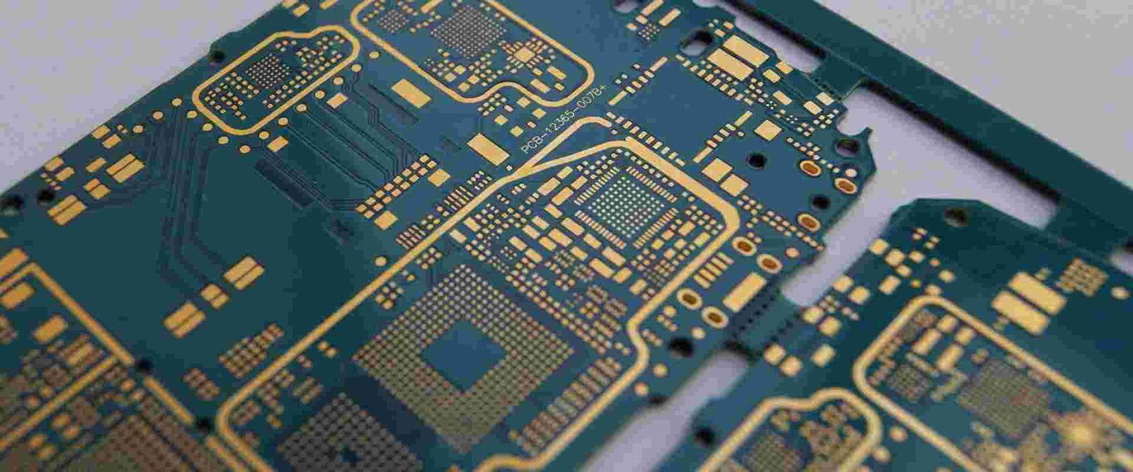
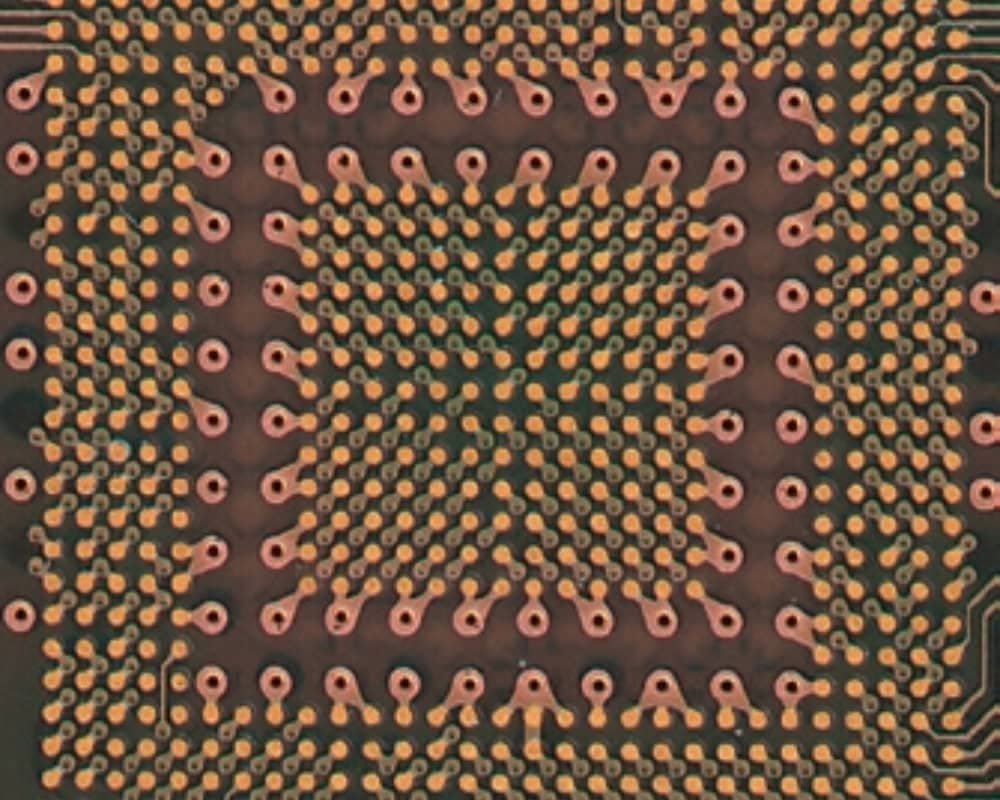
More routing density without simply adding more layers
HDI changes how a PCB uses space. Instead of depending only on full-depth mechanical vias, the design can use laser-drilled microvias and buildup layers to create shorter interconnect paths and more efficient component fanout.
- Support for fine-pitch BGA and area-array components
- More routing flexibility inside compact board outlines
- Shorter via transitions for selected high-speed paths
- Better integration of dense functional blocks
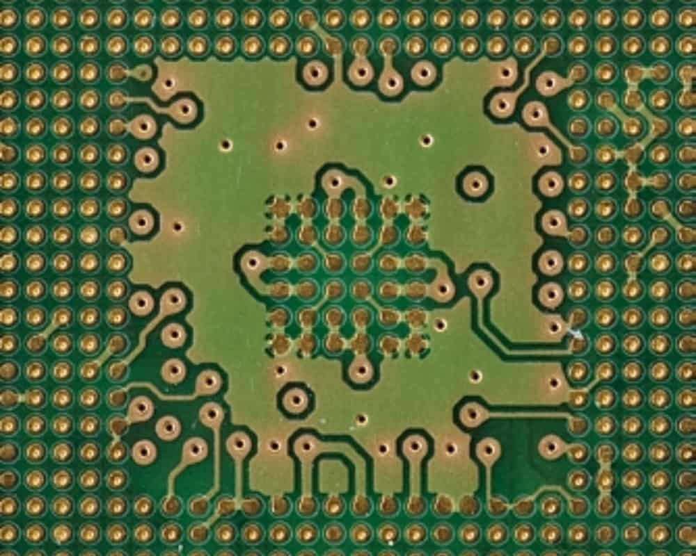
Laser-drilled microvias connect selected adjacent layers within the buildup structure.
Additional dielectric and copper layers are added in controlled buildup cycles.
Stackup, impedance, via strategy and component escape should be reviewed together.
HDI PCB vs. conventional PCB
The right choice depends on component pitch, board size, routing density, electrical performance and production requirements. HDI is not automatically the best option for every design.
| Design factor | Conventional multilayer PCB | HDI PCB |
|---|---|---|
| Main interconnection | Often mechanical plated through-holes | Microvias and buildup, with other vias as required |
| Routing geometry | Agreed for the copper and fabrication process | Finer routing may be evaluated with the approved process |
| BGA escape | Depends on pitch, pad geometry and routing space | Microvia or via-in-pad fanout may enable denser escape |
| Layer count | Selected from routing, power and reference requirements | May decrease, remain unchanged or increase by design |
| Signal transitions | Includes full-depth via and stub considerations | Selected short microvia transitions can be useful |
| Fabrication | Core, lamination, drilling, plating and patterning | May require repeated buildup, drilling and via filling |
| Cost | Construction-specific quotation | Includes the extra process and qualification scope |
On smaller screens, scroll this table horizontally to compare all columns.
These values are design references, not guaranteed production capabilities. Confirm line width, spacing, drill size, annular ring, registration and material limits with your PCB manufacturer before releasing the design.
When should you choose HDI PCB technology?
HDI becomes useful when conventional routing can no longer deliver sufficient component escape, board size, signal integrity or layer efficiency.
Fine-pitch BGA fanout
Choose HDI when BGA pitch and pad arrangement leave insufficient room for conventional dog-bone fanout.
Compact product outline
HDI helps integrate more functions into small products such as portable devices, sensors and embedded modules.
Dense high-speed routing
A carefully planned via structure reduces unnecessary transitions along high-speed paths.
Layer-count optimization
HDI can deliver the required density with a more efficient architecture instead of adding conventional layers.
Compare 1+N+1, 2+N+2 and Any-Layer HDI Stackups
These are architecture examples. Available buildup cycles, via structures and acceptance limits are confirmed for the submitted stackup; this comparison is not a statement of maximum factory capability.
For related construction choices, review Any-Layer HDI, blind vias, buried vias, via-in-pad.
The notation describes buildup layers around an inner-layer structure: N is the inner-layer count, while the outer numbers describe buildup layers on each side. These labels must not be treated as a direct Type I / II / III classification.
Single buildup layer per side
One HDI buildup layer on each side of the conventional core. A practical starting point for moderate density.
- One microvia layer per side
- Suits many standard fine-pitch BGA layouts
- Simplest HDI architecture to control
Two buildup layers per side
Additional buildup layers on each side of the core support more complex fanout and routing transitions.
- More buildup routing options than a 1+N+1 structure
- More microvia routing channels
- Requires detailed stackup coordination
Three buildup layers per side
A more complex buildup configuration for designs that combine multiple microvia layers with dense interconnection.
- Multiple buildup cycles per side
- Used in demanding compact designs
- Higher process and inspection requirements
Microvia interconnect throughout
Microvia-based interconnection is available across the architecture to maximize routing flexibility.
- Maximum routing flexibility
- For highly dense area-array layouts
- Requires strict process qualification
Buildup notation and IPC HDI types are not interchangeable. Altium’s 2+N+2 example describes a Type III architecture; specify the actual layer connections instead of equating Type II with 2+N+2.
HDI PCB Stackup Planning for Density and Reliability
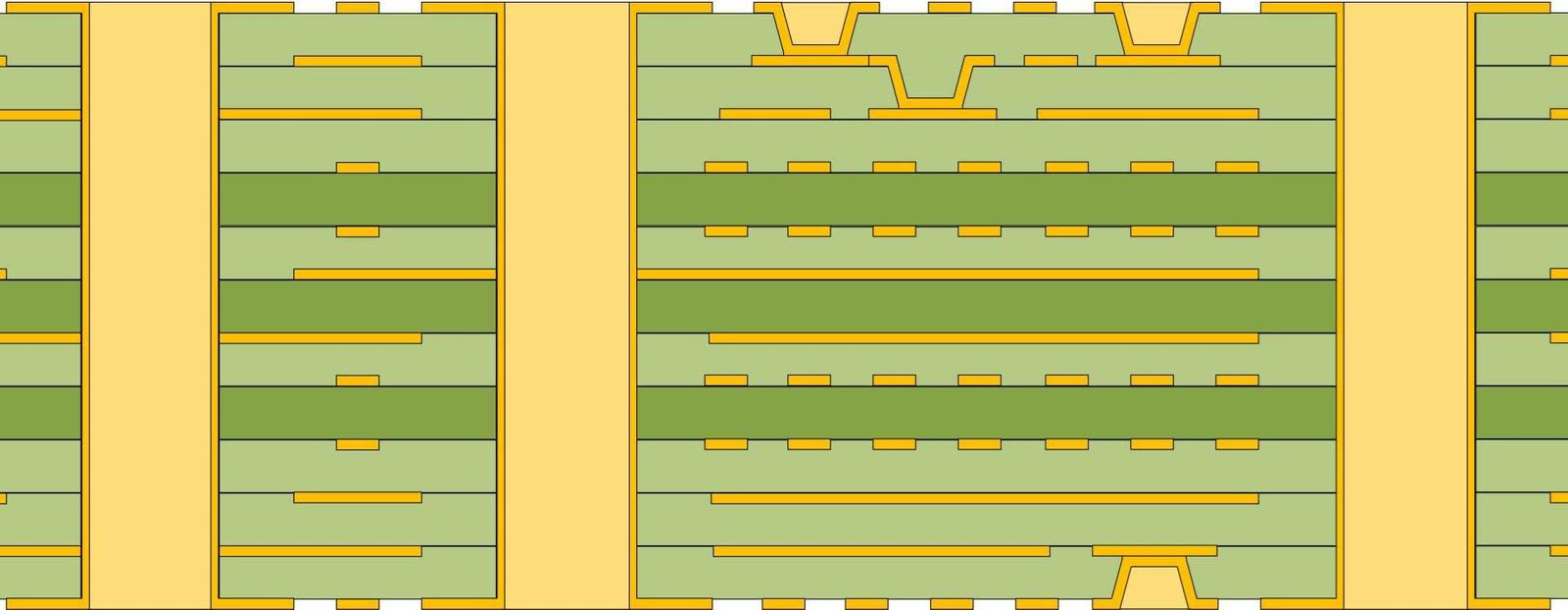
An HDI stackup should be reviewed before routing starts. Dielectric thickness, copper weight, reference planes, microvia depth, impedance targets and lamination sequence all shape the manufacturable result.
Illustrative stackup only. Production stackups are confirmed against the approved material system and impedance requirements.
What should be reviewed before layout?
A manufacturable HDI design is not defined by one microvia dimension. The full buildup architecture must support drilling, lamination, copper fill, registration, electrical test and final assembly.
Define core and buildup layers
Establish core layer count, buildup layers, overall thickness and layer-to-layer connection strategy.
Set impedance targets early
Single-ended and differential targets must connect to trace width, copper thickness and dielectric geometry.
Choose staggered or stacked microvias
The via arrangement affects routing flexibility, copper filling requirements and process complexity.
Check thermal and mechanical constraints
Board thickness, copper distribution and assembly conditions matter as much as routing density.
HDI PCB design rules should be agreed before routing
Use these example targets to start a design discussion, not as GlobalWellPCB capability limits. Confirm the process window, tolerances and inspection requirements before routing.
| Parameter | Example or required input | Engineering review |
|---|---|---|
| Line / space targets | Examples to discuss: 75/75 µm or 50/50 µm | Not confirmed capabilities; depend on copper, layer and process |
| Microvia dimensions | Specify entry diameter, target pad and dielectric depth | Agree drilling, registration and fill requirements |
| Microvia aspect ratio | Define depth divided by the agreed diameter | Confirm the applicable definition and qualified limit |
| Capture pads and annular ring | Provide padstack and registration tolerance | Do not select a universal minimum |
| Controlled impedance | Example targets: 50 Ω single-ended or 100 Ω differential | Use actual interface targets and an approved stackup |
| Via-in-pad | State filled, capped and planarized requirements | Match component pad design and soldering requirements |
| Reliability | Specify stack arrangement and thermal exposures | Agree representative coupons, testing and acceptance |
On smaller screens, scroll this table horizontally to compare all columns.
Microvia and via structures used in HDI PCB design
Different via technologies solve different routing and escape problems. Choosing the simplest structure that meets the requirement helps control risk and manufacturing complexity.
Microvia
A small laser-drilled via that typically connects adjacent layers inside a buildup structure.
Blind via
Connects an outer layer to one or more inner layers without passing through the full board thickness.
Buried via
Connects internal layers and stays inaccessible from the outer surface after lamination.
Via-in-pad
Places a via inside a component pad to improve escape routing. Copper filling and planarization may be required.
Material selection should follow electrical and thermal requirements
Material choice affects signal loss, impedance, thermal performance, reliability, manufacturability and total product cost.
High-Tg FR-4
A practical option for many multilayer and HDI applications that need better thermal stability than standard FR-4 systems.
Low-Loss Materials
Selected when high-speed interfaces, insertion loss, dielectric performance or frequency need tighter control.
Surface Finish Options
The finish should follow fine-pitch assembly, shelf life, solderability, wire bonding and application needs.
From HDI design review to production-ready boards
HDI manufacturing requires coordination between design data, stackup, laser drilling, lamination, via filling, surface finish and inspection.
- 01
Engineering Review
Check files, smallest BGA pitch, layer pairs, impedance and reliability requirements.
- 02
Approve the Stackup
Confirm materials, core and buildup structure, copper and dielectric thicknesses.
- 03
Fabricate the Inner Structure
Form and inspect the core circuitry and any required buried interconnects.
- 04
Laminate a Buildup Layer
Add the approved dielectric and copper in the planned lamination sequence.
- 05
Drill, Metallize and Repeat
Form microvias, complete filling and circuit patterning as specified, then repeat for additional buildup layers.
- 06
Finish, Inspect and Test
Complete surface finish, electrical test and agreed microvia or reliability evidence.
What affects HDI PCB cost?
HDI cost is driven by the full combination of processes, not by layer count alone — buildup complexity, laser drilling, via filling, materials, inspection, board size, volume and yield assumptions all contribute.
HDI buildup layers
Additional buildup layers and any-layer structures increase the number of coordinated fabrication operations. Quote the actual layer and via construction rather than an ambiguous type label.
Laser drilling and via fill
Microvia diameter, aspect ratio, stacked structures and copper-filled via-in-pad requirements change process complexity.
Material and surface finish
High-frequency materials, special finishes and tighter electrical requirements raise total project cost.
Board size and panel utilization
Large boards, unusual outlines, low panel utilization and complex routing reduce manufacturing efficiency.
Volume and yield target
Prototype, pilot and production quantities need different process planning, inspection and yield assumptions.
Testing and documentation
Cross-sections, impedance coupons, special inspection and extra quality records should be included in the RFQ.
For an accurate HDI quotation, submit the complete fabrication package and identify the most critical requirements. Avoid choosing a technology type based only on a target price or layer count.
Where HDI PCB technology is commonly used
HDI is usually selected when product size, component pitch, electrical performance or functional density makes conventional routing difficult.
Compact electronics
Small outlines, dense component placement and fine-pitch packages.
Industrial electronics
Dense control, sensing, communication and embedded architectures.
High-speed products
Controlled impedance, compact routing and careful via transition planning.
What to Ask an HDI PCB Manufacturer
A reliable HDI program depends on process control as well as electrical test. Documentation should make critical dimensions, materials, via structures and inspection results traceable.
Microsection verification
Review buildup thickness, copper connection and via geometry from cross-section evidence.
Dimensional and registration control
Check finished dimensions, pad alignment, layer registration and critical clearances.
Electrical and impedance testing
Continuity and isolation checks do not establish controlled impedance. Agree the electrical-test method separately from impedance coupons, measurement method, tolerance and report requirements.
Production documentation
Keep the approved stackup, fabrication notes, inspection records and revision history aligned.
HDI PCB manufacturing FAQ
Clear answers to common questions about HDI structures, microvias, stackups, design files and manufacturing planning.
What is the difference between an HDI PCB and a standard PCB?
Which HDI stackup should I choose?
Does HDI always reduce the total layer count?
When is via-in-pad required on an HDI PCB?
Can HDI PCBs use FR-4 material?
What information is needed for an HDI PCB quotation?
Technical References and Scope
Explore the material and design references below to compare construction options. Ask us to confirm the selected material, processes and delivery requirements for your design.
- Altium: 2+N+2 HDI stackup and buildup notation
- Isola 370HR: laminate, prepreg and published material properties
Send your material grade, construction, applicable standards and acceptance requirements with your enquiry so we can prepare a quotation for your board.