PCB Thermal
Management
Build a clearer path from heat-generating components to the cooling system. Plan your PCB materials, copper, thermal vias and mounting interface with GlobalWellPCB.
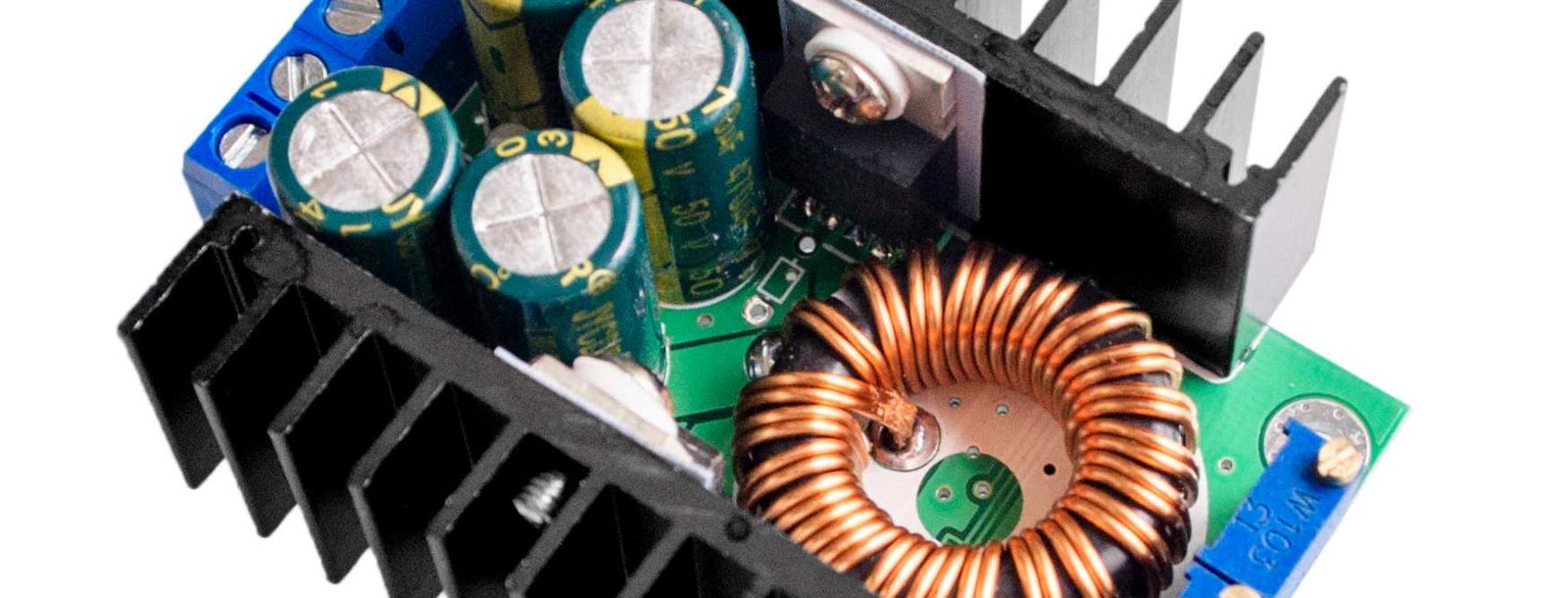
Heat dissipation is a system decision.
PCB thermal management is the coordinated use of layout, conductive paths, substrate materials and cooling interfaces to manage operating temperature. A board can spread heat without providing an adequate route for that heat to leave the assembly.
Start with the heat-generating device, its actual power loss and the available cooling conditions—not a material name alone.
- 01Device junction
The die generates heat under the specified load.
- 02Package & solder
The intended thermal pad couples the device to the board.
- 03PCB structure
Copper, vias and the substrate carry and spread heat.
- 04Mounting interface
The thermal interface connects the board to its cooler.
- 05Heat rejection
A sink, chassis or cold plate transfers heat onward.
This is an explanatory path, not a universal stackup. Top-cooled packages and parallel heat paths require different models. The interfaces and boundary conditions must match the actual assembly.
Choose a thermal solution.
Not just a higher conductivity.
Compare thermal-management options by heat source, cooling conditions and insulation needs, then confirm the construction for your design.
Listed constructions are design candidates. Material availability, processing limits and acceptance criteria require project-specific confirmation.
| Construction | Thermal role | Potential project fit | Review before release |
|---|---|---|---|
| FR-4 with copper planes & thermal vias | Uses copper to spread heat and vias to connect layers. | Multilayer control, mixed-signal and power designs that need routing flexibility. | Check usable copper area, via connections and the final heat-rejection path. |
| Heavy copper PCB | Adds conductor cross-section for current paths and lateral heat spreading. | Power distribution and layouts where copper loss is a significant contributor. | Review trace geometry, copper balance and assembly heating; thicker copper alone does not bypass dielectric. |
| Aluminum or copper-base IMS | Combines circuit copper, an insulating dielectric and a metal base. | LED and power assemblies with a defined board-to-sink interface. | Specify dielectric thickness, insulation requirements, base alloy and mounting details together. |
| Ceramic substrates: DBC / AMB | Provides a ceramic insulating layer with bonded or brazed copper. | Power-module concepts requiring a ceramic thermal and mechanical construction. | Choose the ceramic and bonding system as a set; confirm geometry, reliability criteria and build availability. |
Scroll the table horizontally to compare all four columns.
Need a copper coin, insert, cavity or selective direct-to-metal feature? Include the mechanical drawing, electrical isolation intent and interface details in your RFQ so the proposed construction can be assessed separately.
Resin-filled vias retain a plated copper barrel; the resin fill is distinct from the copper conductor.
Thermal vias need a destination.
An array is only useful when its connections form a practical heat path. Start with the package requirements, then resolve the board and assembly details.
Follow the device’s electrical requirements
Check the exposed-pad land pattern and required electrical potential. A thermal pad must not be assigned to ground simply because it carries heat.
Describe the actual via construction
A plated barrel, resin-filled and copper-capped via, and copper-filled via are not the same structure. Non-conductive fill is not a solid-copper heat path; the barrel still provides conduction.
Coordinate with soldering and fabrication
Review finished hole size, plating, pitch, via count, connection layers and fill/cap requirements together. Package guidance and solder-wicking or voiding risks matter more than a universal “vias per watt” rule.
Material properties are not
finished-board performance.
Compare the dielectric and ceramic material examples by their stated test conditions. Confirm the exact grade and complete board construction for your thermal design.
| Supplier / material | Typical k | Published basis |
|---|---|---|
| Ventec VT-4B3 IMS dielectric | 3.0 | ISO 22007-2; dielectric property. |
| Rogers curamik Power Alumina / Al₂O₃ | 24 | Ceramic value at 20°C; DBC construction. |
| Rogers curamik Thermal Aluminum nitride / AlN | 170 | Ceramic value at 20°C; DBC construction. |
| Rogers curamik Performance Silicon nitride / Si₃N₄ | 90 | Ceramic value at 20°C; AMB construction. |
Scroll horizontally to see the test basis.
Values are supplier-published examples reviewed on 14 September 2026. Confirm the current grade, measurement direction, temperature, thickness and datasheet revision before selection.
For an ideal uniform layer, Rth = t / (k × A). Thickness and contact area matter alongside conductivity. This approximation omits spreading and contact resistance.
- Conductivity k · W/(m·K)
- A material property. It does not include all the interfaces and geometry of an assembly.
- Thermal resistance · K/W
- A temperature difference per unit heat flow for a defined path. Area-normalized impedance uses additional area units.
- Glass transition Tg · °C
- A separate polymer property, not a conductivity rating or a universal continuous-use temperature. The VT-4B3 datasheet lists Tg, conductivity and maximum operating temperature separately.
Set a thermal
resistance budget.
Translate a temperature target and device power loss into an allowable effective junction-to-ambient resistance. This sets a requirement; it does not show that a board can achieve it.
Use dissipated heat, not rated output power. The simple steady-state relationship does not resolve multiple heat sources or pulsed operation; those require an appropriate thermal model.
Datasheet θJA depends on test-board and environmental conditions. Do not add it to a heat-sink resistance as though it were a package-only series element. Use compatible thermal boundaries and parameters.
Thermal budget calculator
The initial values are an illustration, not recommended operating limits. Select a junction target from the device requirements with an appropriate design margin.
The mounting interface
deserves its own review.
A higher-conductivity substrate cannot remove an interface bottleneck by itself. Include the actual board-to-sink arrangement in the design package.
Thermal interface material performance depends on the installed bond line and contact conditions. A bulk conductivity number alone is not enough to rank an interface.
- Contact and clamping
- Specify mating surfaces, flatness requirements, screw locations, permitted board deflection and the intended assembly pressure.
- Interface and insulation
- Identify the TIM grade, installed thickness or compressed gap, electrical isolation intent and any interface qualification requirements.
- Cooling boundary conditions
- Document enclosure temperature, airflow, orientation and the heat-sink or cold-plate conditions used for evaluation. These are part of the model, not background details.
- Operating profile
- State continuous load, pulse duration, duty cycle, startup events and simultaneously active heat sources. Do not replace a transient requirement with an average-power assumption without review.
Define what the prototype
needs to prove.
Separate bare-board acceptance from powered-assembly thermal validation. Define both scopes before ordering; neither should be assumed from a material datasheet.
Bare-board requirements
Request the agreed stackup, material identification, copper and via-plating checks, electrical test and dimensional inspection. Include microsection or insulation-test requirements where needed.
Powered-assembly requirements
Agree the load case, cooler, ambient condition, measurement locations, stabilization criterion and reporting method. Package-surface temperature is not automatically junction temperature.
- 01 / DEFINE
Capture the limits
Record device loss, temperature targets, cooling conditions and isolation requirements.
- 02 / REVIEW
Resolve the construction
Align materials, stackup, copper, vias and mounting details in the fabrication package.
- 03 / VALIDATE
Evaluate the prototype
Compare the agreed operating test results with the defined acceptance criteria.
- 04 / RELEASE
Control the revision
Document the approved build, assembly interface and permitted changes before repeat production.
Thermal simulation, powered testing, thermal cycling and specialized inspections are separate scope items. Confirm responsibility, availability and deliverables in writing.
PCB thermal
management FAQs
The distinctions that help turn a general cooling request into an actionable board specification.
Can an FR-4 PCB provide useful thermal management?
Yes. Copper planes and thermal vias can contribute to heat spreading and transfer. Whether the assembly meets its limits depends on loss, geometry and cooling—not on the FR-4 label alone.
Does a metal-core PCB eliminate the need for a heat sink?
No automatic conclusion follows from the metal base. Review how heat leaves the assembly and assess whether the available surfaces, chassis or dedicated cooler can meet the operating target.
Is a high-Tg PCB the same as a high-conductivity PCB?
No. Glass transition, thermal conductivity and maximum operating temperature are distinct properties. Review the specified material grade and the full thermal construction instead of using Tg as a heat-dissipation rating.
Are resin-filled, copper-capped vias the same as copper-filled vias?
No. Resin fill and a copper cap do not turn the entire hole into solid copper. State the fill material, plating and cap requirements explicitly so the thermal model and fabrication instructions describe the same structure.
How many thermal vias are required?
There is no universal count per watt. The package land pattern, via geometry, connected copper, board thickness and assembly constraints determine the appropriate array.
Can I predict my PCB temperature using datasheet θJA?
Not without checking the conditions. Datasheet θJA includes the influence of its test board and environment. An application-specific estimate requires matching assumptions or a suitable model, followed by validation.
What is needed for a thermal management PCB quote?
Provide fabrication and drill data, the stackup and drawings, quantity and revision, plus device-loss information, temperature targets and cooling details. Mark any material, via-fill, insulation or validation requirement that must be confirmed.
Continue the engineering review.
Technical references & scope
Use the supplier documents below to compare thermal materials and construction options. Send your requirements to confirm the materials, processes and tests for your quotation.
- [1]Texas Instruments — PowerPAD™ Thermally Enhanced Package, SLMA002HExposed pads, thermal via layout and soldering considerations; Rev. H, July 2018.
- [2]Texas Instruments — Semiconductor and IC Package Thermal Metrics, SPRA953DThermal parameter definitions and test-condition limitations; Rev. D, March 2024.
- [3]Analog Devices — Maximize Power Capability in Thermal Design, Part 1Heat-transfer modes and steady-state temperature / power / resistance relationships.
- [4]Analog Devices — Layout Considerations for High-Power CircuitsCopper paths, heat spreading and PCB layout.
- [5]Ventec — VT-4B3 Metal Base Laminate datasheetDielectric conductivity, thickness-dependent impedance and separate Tg / MOT properties; version 23 August 2023.
- [6]Rogers — curamik ceramic substrate product dataPublished ceramic conductivity values at 20°C; see the individual construction pages below.Individual pages: Power / Al₂O₃ · Thermal / AlN · Performance / Si₃N₄
- [7]Henkel — Thin-bond-line thermal interface material technical releaseRelationship between bond line, pressure and thermal interface performance; 16 May 2023.
- [8]Analog Devices — Exposed Pads: A Brief IntroductionPackage land pattern and electrical-potential requirements.
- [9]Analog Devices — ADPA9002 / HMC8410 via-treatment FAQDevice-specific example distinguishing epoxy fill, copper barrels and copper overplating—not a universal via specification.
- [10]Analog Devices — AN-1604: Thermal Management Calculations for RF AmplifiersDefined thermal paths, layer resistance and conduction through a PCB assembly.
- [11]Analog Devices — SOAtherm PCB and Heat-Sink Thermal ModelsTransient and steady-state behavior, geometry and cooling boundary conditions.
Technical content reviewed: 14 September 2026. All calculations on this page are preliminary planning aids, not thermal simulation or product qualification.