Copper Base PCB
A copper foundation for heat-intensive electronics.Plan your copper-base PCB around the complete thermal path. Bring the substrate, electrical insulation, component footprint and heat-sink interface into one manufacturing brief.
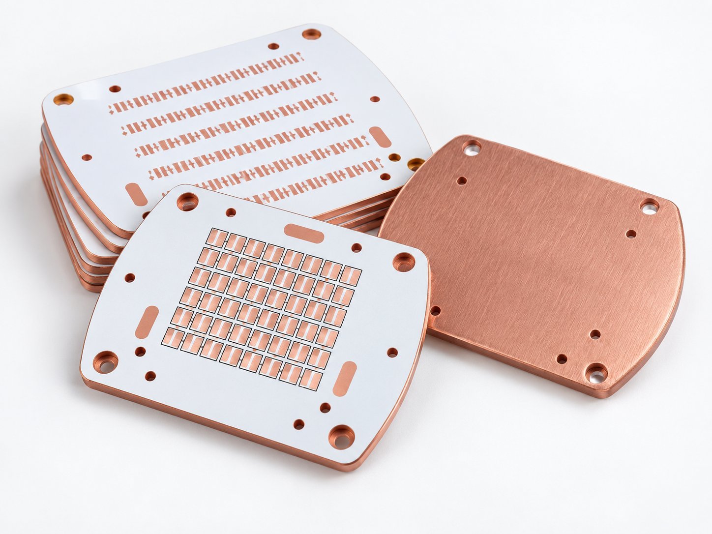
What is a copper base PCB?
For related construction choices, review aluminum-base PCB, heavy-copper PCB.
A copper base PCB is a metal-base printed circuit board that uses a solid copper substrate beneath its circuitry. In a conventional insulated metal substrate (IMS), a thermally conductive dielectric electrically separates the patterned copper foil from the base.
The base provides a path for heat spreading and mechanical support. It is not the same layer as the etched conductors that connect components. Aismalibar’s copper-base laminates illustrate this distinction: a copper base on one side, and circuit copper foil on the other.
One base material.
Two different thermal paths.
Confirm the component footprint and insulation requirements before selecting a construction.
Insulated copper-base PCB
The circuit copper sits above a continuous insulating dielectric bonded to the copper base. Heat crosses that dielectric before entering the base.
Component → circuit pad → dielectric → copper base
Review the dielectric grade, finished thickness, insulation target and contact area as part of the same thermal design.
Direct thermal path copper PCB
A designated thermal pad bonds to an exposed copper feature, bypassing the dielectric locally. This is a different stackup—not a claim that the entire board is electrically uninsulated.
Compatible thermal pad → solder joint → copper base
Check the package’s thermal-pad electrical connection first. Cree LED’s XE-G is one published example of an isolated pad supporting a direct thermal path.
Copper base PCB vs aluminum base PCB
Compare identified alloys—not one generic conductivity number for every copper or aluminum board.
Scroll horizontally to compare all columns.
| Property | Copper C1100 | Aluminum 5052H32 | Aluminum 6061T6 |
|---|---|---|---|
| Thermal conductivity | 386 W/m·K | 138 W/m·K | 167 W/m·K |
| Density | 8.9 g/cm³ | 2.7 g/cm³ | 2.7 g/cm³ |
| Selection question | Does improved base spreading justify the added mass? | Does this alloy meet the thermal and mechanical brief? | Are this alloy’s properties and machining needs a better fit? |
Supplier values are typical, not acceptance limits. Confirm the selected grade and conditions. Different base materials do not by themselves determine the performance of the complete assembly.
Compare the complete thermal route
For a meaningful project comparison, hold the geometry, heat load, mounting and test conditions consistent. Evaluate the dielectric, solder joint, thermal interface material and heat sink—not only the base metal.
Do not substitute a current-carrying specification
A copper substrate and a heavy-copper conductor solve different parts of the design. Where current is the main concern, include trace width, finished copper and interconnect requirements in the review.
A copper number is not
a board temperature.
Metal conductivity describes a material. Thermal resistance describes a defined path. The calculation beside this text illustrates why dielectric thickness and contact area matter even when the base stays unchanged.
- Identify what was measured
Ask whether the reported value belongs to the dielectric, base metal, laminate or assembled product.
- Define the heat-sink interface
Document the contact surface, flatness, thermal interface material, mounting arrangement and cooling conditions.
- Validate the complete product
Set the operating load and temperature acceptance points. Do not treat a single-layer calculation as a junction-temperature prediction.
Dielectric-only thermal resistance
Illustrative one-dimensional conduction model: R = t ÷ (k × A).
Assumes steady, uniform through-thickness heat flow with constant k. Excludes spreading, contact resistance, solder, copper, the package and heat sink. Input values are examples, not material selections or manufacturing limits.
Define the build before
choosing a capability number.
Include these copper-base construction details with your enquiry so we can confirm materials, dimensions and inspection requirements.
Scroll horizontally to view the full requirements checklist.
| Parameter | What to specify | Useful supporting information |
|---|---|---|
| Construction & layer count | Insulated IMS, DTP or a proposed custom stackup; number of circuit layers. | A cross-section identifying the function of every layer. |
| Copper base | Requested grade, base thickness, finished outline and allowable tolerances. | Mechanical drawing; identify whether the base is isolated, grounded or electrically connected. |
| Circuit copper | Finished conductor thickness, trace/space requirements and critical current paths. | Fabrication data and copper notes separate from the base-plate specification. |
| Dielectric system | Supplier grade, thickness, conductivity test method and insulation requirements. | Approved material data; identify permitted substitutions and approval rules. |
| Thermal pad / DTP feature | Component part number, thermal-pad connection, footprint and mating height. | Package drawing, copper-feature drawing and electrical isolation review. |
| Holes, slots & mounting | Plated or non-plated holes, insulation to the base, edge clearance and mounting face. | Drill data plus clear definitions of holes that may contact the metal. |
| Finish & assembly | Pad finish, mask openings, base-surface treatment and assembly scope. | Assembly drawing, BOM and placement data when assembly is requested. |
| Acceptance & delivery | Inspection, isolation tests, thermal validation, quantity and requested date. | Written acceptance criteria and a quotation confirming feasibility and schedule. |
Published material examples—not a stock list
Aismalibar’s COBRITHERM HTC Copper Base family lists 2.2 W/m·K dielectrics at 75 or 130 µm, and a 3.2 W/m·K option at 100 µm. Ventec’s VT-4B7 literature lists a 7.0 W/m·K dielectric with 75, 100 and 150 µm options.
These figures describe supplier materials, not GlobalWellPCB inventory, approved substitutions or the effective conductivity of a finished board. Request the exact grade and construction in the quotation.
Resolve the details
that connect heat and hardware.
Ask for the review and inspection scope to be confirmed before production release.
Thermal-pad compatibility
Check the pad’s electrical function, package drawing and base potential. Include any DTP height and coplanarity requirements rather than relying on a package-family name.
Insulation & exposed metal
Specify the isolation between circuitry and the base, including holes and edges. Define proof-test voltage, AC or DC, duration and acceptance criteria; do not substitute a breakdown value.
Mounting & assembly
Agree the mounting face, flatness, interface material and assembly process. Ask for the actual board’s soldering profile to be reviewed rather than assuming an FR-4 profile transfers unchanged.
Inspection & evidence
Request the agreed continuity/isolation checks, dimensional inspection and any cross-section evidence. Treat product thermal testing as a separate, explicitly defined validation activity.
Thermal evaluation should record the assembly configuration, load and cooling conditions.
Inspection records should identify the board revision, method and acceptance criteria.
Match the substrate
to the actual heat source.
Metal-base laminate literature identifies lighting, power conversion and motor-drive applications. Suitability still needs project-level review.
High-power LED modules
What are the package part numbers, thermal-pad connections, power dissipation and available heat-sink area? Does the layout call for an insulated or direct thermal path?
Power conversion stages
Which devices dominate the heat load? Define their loss estimates, electrical potentials, insulation needs and the complete cooling arrangement.
Motor drives & controllers
What are the duty cycle, ambient conditions and mounting constraints? Coordinate the thermal design with the current paths and system isolation.
A clear route to
a manufacturing-ready brief.
- 01
Share the package
Provide fabrication data, the proposed stackup, component details, mechanical drawings, quantity and revision.
- 02
Review open decisions
Resolve substrate grade, insulation, DTP suitability, hole construction, assembly scope and required evidence.
- 03
Approve the build
Approve the quoted construction, substitutions, drawing changes, test plan and schedule before release.
- 04
Verify the agreed scope
Review the specified records and handle deviations explicitly. Retain the approved configuration for repeat orders.
Copper Base
PCB FAQs
Clarify the construction before committing to a material, layout or purchase specification.
Is copper base PCB the same as heavy copper PCB?
No. Copper base describes the solid metal substrate. Heavy copper describes thicker circuit conductors, which may be built into FR-4 multilayers. State both requirements when a design needs both.
Does every copper-base PCB use a direct thermal path?
No. Conventional insulated constructions retain a dielectric between the circuit foil and base. DTP bypasses that layer locally beneath a designated thermal pad.
Can any LED be placed on a DTP copper PCB?
Do not assume so. Verify the exact package drawing, thermal-pad electrical connection and insulation scheme. An isolated-pad package such as Cree LED’s XE-G illustrates the relevant distinction; it does not establish compatibility for every LED.
Is 386 W/m·K the thermal conductivity of the whole PCB?
No. The cited value describes C1100 copper in Ventec’s metal-plate table. It is not a finished-board or junction-to-ambient rating. Define the actual thermal path and test conditions.
Is a copper base always preferable to aluminum?
Not automatically. Compare the complete construction against the heat load, mechanical envelope, mass target and quoted cost. The decision should follow a consistent thermal and mechanical evaluation.
Can a copper-base PCB include multiple circuit layers?
Metal-base PCBs can use more than one circuit layer, but the routing, interconnects and insulation need a defined stackup. Treat a multilayer copper-base request as a project-specific engineering review, not an assumed standard build.
What base thickness, finish and lead time are available?
They must be confirmed against the actual design and quotation. Include your requested dimensions, tolerances, finish, quantity and target date. No fixed stock range or delivery promise is implied by this page.
What files should I prepare for a quotation?
Prepare the fabrication data and drill files, an outline drawing, proposed cross-section, component thermal-pad details and acceptance requirements. Include BOM and placement data for assembly, and distinguish base thickness from circuit-copper thickness.
Related PCB planning
Technical references & scope
Explore the material and construction references below. Your quotation will confirm the copper-base construction, materials and testing available for your board.
- [1] Aismalibar — COBRITHERM HTC constructionInsulated metal substrate construction and the roles of the base, dielectric and circuit foil.
- [2] Aismalibar — COBRITHERM HTC Copper BaseCopper-base laminate family and published dielectric conductivity / thickness examples.
- [3] Ventec — VT-4B7 technical dataTypical alloy properties, dielectric data, applications and the distinction between proof and breakdown testing.
- [4] Multi Circuit Boards — Thermal management for Printed Circuit BoardsThicker circuit copper in FR-4 constructions; a different design choice from a solid copper base.
- [5] Cree LED — XLamp XE-G LEDsAn electrically isolated thermal-pad example supporting a direct thermal path.
- [6] Andwin Circuits — Direct Thermal Path MCPCBIllustration of a dielectric bypass beneath the thermal pad. Performance and compatibility claims are not adopted as universal guarantees.