GlobalWellPCBPCB & PCBA Manufacturing
01 / Ceramic PCB

Ceramic PCB Manufacturing

Explore ceramic PCB options for your electrical and thermal requirements. Compare alumina, aluminum nitride and other substrates, and send your design to discuss metallization and inspection needs.

  • 01 Alumina and AlN material options
  • 02 Thermal and high-power design review
  • 03 Prototype-to-production engineering support
02 / Definition

What Is a Ceramic PCB?

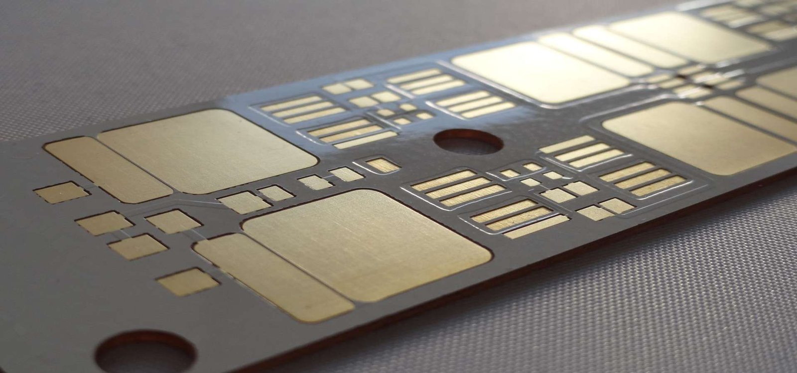
Ceramic PCB refers to a circuit board or ceramic circuit substrate that uses a ceramic material as the base instead of a conventional resin laminate.

The substrate, conductor system and interconnect method should be selected together.
Quick answer

A ceramic PCB uses an alumina, aluminum nitride or other ceramic substrate to support conductive traces, pads and interconnects. Compared with FR-4, ceramic construction is considered when heat dissipation, temperature stability, insulation performance or mechanical reliability requires a different material system.

01 / THERMAL

Thermal Management

Ceramic substrates can provide a direct thermal path for designs where heat spreading and component temperature are important.

02 / TEMPERATURE

Temperature Stability

Ceramic material systems are evaluated for applications exposed to elevated temperature, thermal cycling or demanding environments.

03 / INSULATION

Electrical Insulation

The ceramic substrate can combine electrical insulation with a conductive metallization structure on the circuit side.

04 / RELIABILITY

Dimensional Reliability

Material selection and process control are important when the design requires stable geometry, thermal cycling performance or controlled interfaces.

03 / Material Selection

Alumina PCB, AlN PCB and Silicon Nitride Materials

Alumina, aluminum nitride and silicon nitride serve different engineering priorities. The correct choice depends on thermal load, electrical behavior, mechanical stress, thermal expansion and cost target.

Al2O3 Alumina

Alumina Ceramic PCB

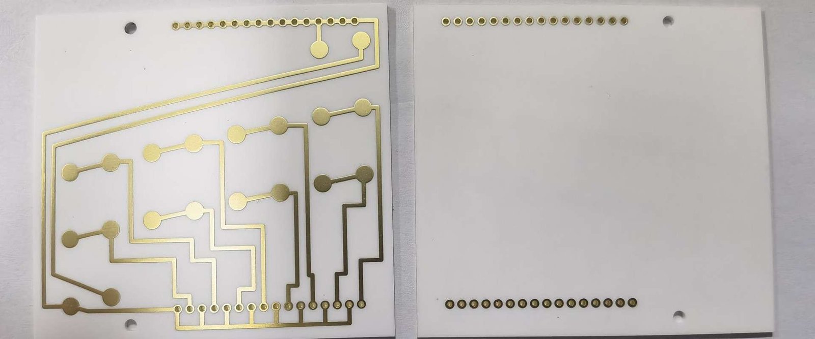
Alumina is often used as a balanced ceramic substrate for electrical insulation, temperature performance and cost. It can be considered for sensors, LED designs, industrial electronics and general ceramic circuit applications.

Balanced material option
AlN Aluminum Nitride

Aluminum Nitride PCB (AlN)

Aluminum nitride is considered when thermal conductivity and semiconductor interface behavior are major design factors. It is commonly evaluated for power electronics, high-power modules and thermally demanding assemblies.

Thermal-focused material option
Si3N4 Silicon Nitride

Silicon Nitride Ceramic

Silicon nitride can be considered for designs where mechanical toughness, thermal cycling and demanding power or industrial environments are important.

Mechanical reliability option
Published Ceramic Material Examples

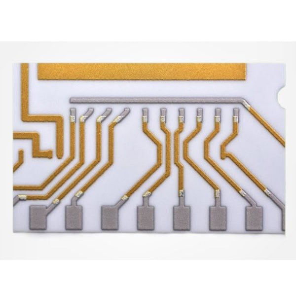
Rogers lists thermal conductivity at 20°C of 24 W/m·K for curamik Power alumina, 170 W/m·K for curamik Thermal AlN and 90 W/m·K for curamik Performance silicon nitride. These are specific supplier examples, not universal ceramic values, GlobalWellPCB stock commitments or finished-board thermal resistance ratings.

Sources: alumina, AlN and silicon nitride.

04 / Circuit Construction

DPC, DBC and Other Ceramic PCB Construction Methods

Ceramic PCB construction is not defined by the substrate alone. The conductor thickness, via structure, circuit geometry and metallization method all influence manufacturability and application performance.

Direct Plated Copper

DPC Ceramic PCB

Direct plated copper construction can be evaluated for patterned copper circuits, controlled geometries and applications requiring a ceramic-to-metal interface.

Direct Bonded Copper

DBC Ceramic Substrate

Direct bonded copper is commonly considered for power-oriented designs where thicker copper structures and thermal paths are important.

Printed Conductor

Thick-Film Ceramic

Thick-film construction uses printed conductive or resistive layers and can be suitable for robust ceramic circuits, sensors and hybrid electronic structures.

Fine Pattern

Thin-Film Ceramic

Thin-film construction can be considered when fine circuit features, controlled metallization and compact geometries are important.

Active Metal Brazing

AMB Ceramic Substrate

AMB joins copper to ceramic using an active braze system. Silicon nitride constructions are evaluated for demanding power and thermal-cycling applications.

Technology reference, not a list of confirmed factory processes. Rogers describes DBC and AMB as distinct joining routes. Confirm the ceramic, copper thickness, geometry and process availability before ordering.

05 / Material Comparison

Ceramic PCB vs. FR-4 and Metal Core PCB

Ceramic PCB is not automatically the best choice for every design. The decision should be based on thermal requirements, electrical isolation, operating environment, mechanical constraints and total project cost.

Ceramic PCB vs. FR-4 and Metal Core PCB
Design Factor Ceramic PCB FR-4 PCB Metal Core PCB
Substrate system Alumina, AlN, silicon nitride or another ceramic system. Resin laminate reinforced with glass fiber. Metal base combined with an electrically insulating dielectric layer.
Thermal design Selected when the ceramic substrate and metallization structure need to support heat spreading. Suitable for many general electronic designs; thermal performance depends on construction and external cooling. Often considered for LED and power designs where a metal base helps conduct heat.
High-temperature use Can be evaluated for elevated-temperature or thermal-cycling environments. Depends on the selected laminate grade and operating conditions. Depends on dielectric system, metal base and assembly environment.
Electrical insulation Ceramic provides an insulating substrate with conductive metallization on the circuit side. Built-in dielectric laminate structure supports standard PCB insulation requirements. Requires control of the dielectric layer between copper and metal base.
Typical decision driver Thermal performance, temperature stability, insulation and reliability requirements. General electronics, broad manufacturability and cost-sensitive designs. Thermal management for selected LED, power and mechanical form-factor designs.

On smaller screens, scroll this table horizontally to compare all columns.

06 / Applications

Where Ceramic PCBs Are Considered

Ceramic circuit boards are usually evaluated when the substrate must perform more than a basic electrical routing function.

Power Electronics

Power modules, switching devices and high-current structures where thermal paths and insulation need to be reviewed together.

LED and Laser Systems

LED drivers, laser packages and light-source assemblies where heat dissipation can influence component performance.

RF and Microwave

RF, microwave and high-frequency assemblies that require a controlled substrate and stable circuit geometry.

Industrial Sensors

Sensors and instrumentation exposed to temperature variation, vibration or demanding operating environments.

Automotive Electronics

Selected automotive power and sensing designs where temperature, reliability and packaging constraints are important.

Medical and Instrumentation

Compact electronic assemblies that require electrical insulation, dimensional stability and controlled material selection.

07 / Manufacturing Flow

From Ceramic Material Selection to Validated Circuit

The production flow varies according to the selected ceramic, metallization system, conductor thickness, via structure and final assembly requirements.

  1. 01

    Design Intake

    Review the application, electrical targets, thermal load, material preference, quantity and project stage.

  2. 02

    Material Review

    Compare alumina, AlN or another ceramic system against thermal, mechanical, electrical and cost requirements.

  3. 03

    Circuit Formation

    Define the appropriate DPC, DBC, thick-film or thin-film construction for the required circuit pattern.

  4. 04

    Finishing and Inspection

    Complete surface treatment, dimensional checks and electrical or visual inspection according to the project plan.

  5. 05

    Prototype to Production

    Use prototype findings to refine the drawing, acceptance criteria, assembly interface and repeat-production plan.

08 / Engineering Data

What to Prepare Before Requesting a Quote

The more complete the design data, the easier it is to select the material and manufacturing route without creating assumptions.

A preliminary quotation can begin with incomplete data, but final confirmation requires reviewed drawings and specifications.

Recommended Project Information

  • 1
    Fabrication data Gerber, ODB++, IPC-2581, DXF or equivalent design files.
  • 2
    Material preference Alumina, AlN, silicon nitride or an application-based material recommendation.
  • 3
    Copper or metallization requirements Conductor thickness, pattern geometry, pad structure and surface finish requirements.
  • 4
    Mechanical requirements Overall dimensions, thickness, flatness, edge features, holes, slots and tolerances.
  • 5
    Validation requirements Electrical tests, visual inspection, dimensional reports, thermal testing or assembly validation.

Technical Review Checklist

Expand construction and acceptance checks
Ceramic material
Alumina, AlN, silicon nitride or another specified ceramic system.
Construction method
DPC, DBC, thick-film, thin-film or another reviewed interconnect method.
Conductor structure
Defined by circuit geometry, current, thermal load, bonding method and assembly interface.
Surface treatment
Specified according to the metallization system, soldering process and application environment.
Dimensional control
Board size, thickness, flatness, holes and edge tolerances confirmed by drawing.
Inspection plan
Visual, dimensional, electrical or functional checks aligned with project acceptance criteria.
09 / Quality Planning

Choosing a Ceramic PCB Manufacturer

Ceramic PCB reliability depends on material selection, conductor design, thermal interface, dimensional control and assembly conditions. These items should be reviewed before the first build.

Expand material and inspection planning
Material traceability Confirm the selected ceramic material and relevant documentation before production.
Drawing alignment Review dimensions, tolerances, conductor geometry, holes and edge features against the latest drawing.
Thermal interface review Evaluate the substrate, copper structure, component interface and cooling path as one system.
Inspection planning Define visual, dimensional, electrical and functional checks according to the application.
Assembly compatibility Confirm soldering, bonding, wire bonding, attachment and downstream assembly conditions.
Prototype learning Use first-build results to refine tolerances, materials and production acceptance criteria.
10 / FAQ

Ceramic PCB Frequently Asked Questions

Clear answers to common material, design and quotation questions.

What is a ceramic PCB?

A ceramic PCB is a circuit board built on a ceramic substrate such as alumina or aluminum nitride. The ceramic substrate is selected when thermal management, high-temperature stability, electrical insulation or dimensional reliability is important.

What is the difference between alumina PCB and AlN PCB?

Alumina is often selected as a balanced ceramic substrate for electrical insulation, temperature performance and cost. Aluminum nitride is considered when higher thermal conductivity and semiconductor-compatible thermal expansion behavior are important.

Can ceramic PCBs be used for high-power applications?

Ceramic PCBs are commonly evaluated for high-power and power-electronic designs because ceramic substrates can support thermal spreading, electrical insulation and temperature stability. Final suitability depends on material, copper structure, power density and thermal design.

What files are needed for a ceramic PCB quotation?

A quotation normally benefits from Gerber, ODB++, IPC-2581 or equivalent fabrication data, together with drawings, material requirements, copper thickness, quantity, testing requirements and target delivery information.

Can ceramic PCBs be multilayer?

Multilayer ceramic circuit structures are possible, but the construction depends on the selected ceramic system, conductor technology, via design, layer count and manufacturing process. The stackup should be reviewed before production.

How do I start a ceramic PCB project?

Start by sharing the design files, application, preferred ceramic material, quantity, copper or metallization requirements and target schedule. An engineering review can then confirm the material and manufacturing route.

Technical References and Scope

Explore the material and design references below to compare construction options. Ask us to confirm the selected material, processes and delivery requirements for your design.

Send your material grade, construction, applicable standards and acceptance requirements with your enquiry so we can prepare a quotation for your board.

Scroll to Top