PCB fabrication
- Gerber or ODB++ fabrication data and the board outline
- Layer stackup, material identity, finished copper and board thickness
- Drill data, impedance targets, surface finish and inspection requirements
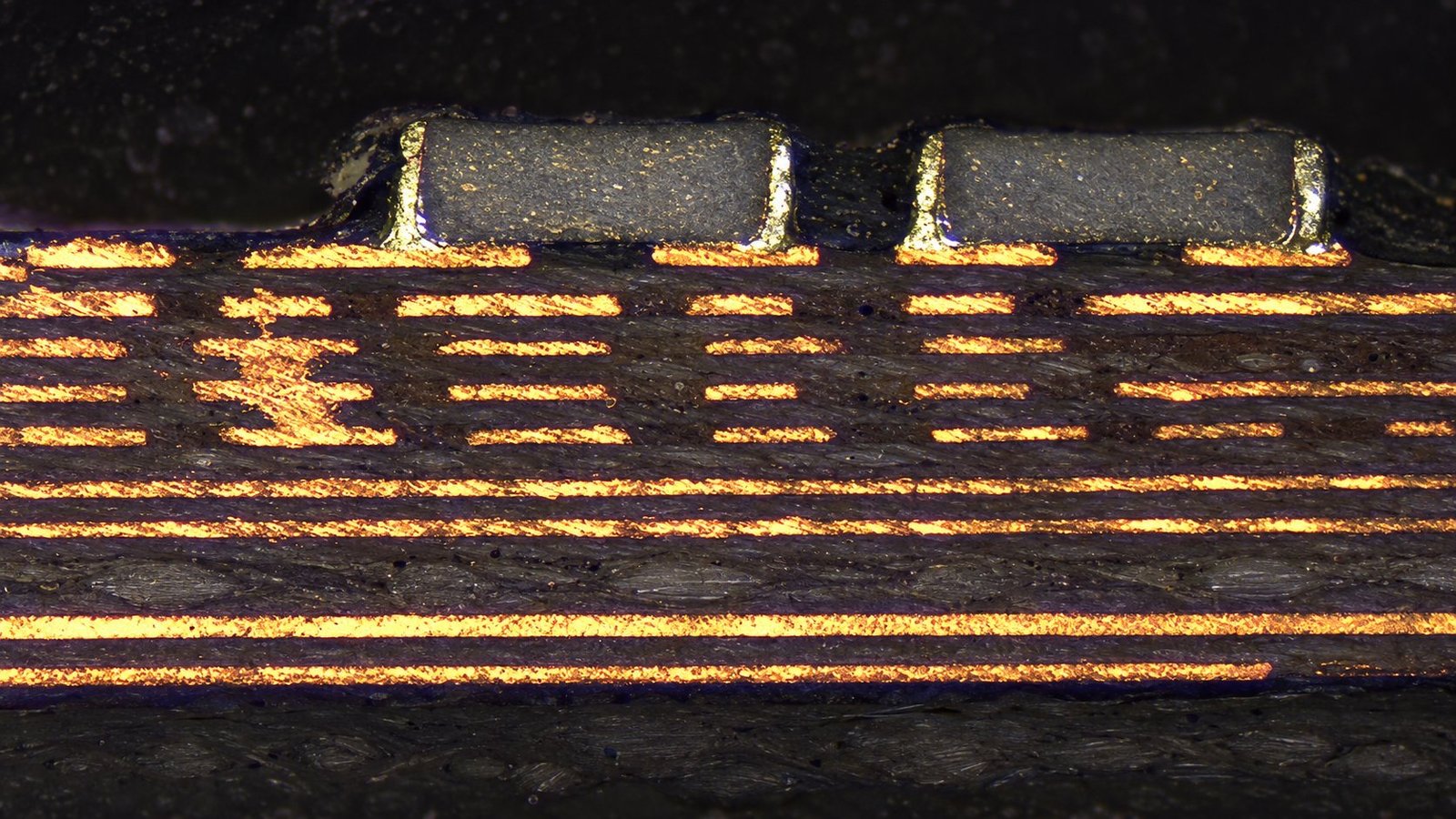
A released stackup links layer order, material identity, copper and dielectric thickness to the via map and controlled signals. Use the layer-count references as planning discussions, then release a construction that matches the actual electrical and mechanical requirements.
Read each value together with its board type and review conditions.
Published limits apply to their stated board type. Layer count, copper weight and minimum geometry require a combined engineering review.
Show both the nominal construction and the requirements that engineering may or may not adjust.
On smaller screens, scroll within the table to see every column.
| Parameter | Published capability | Applies to | Review conditions |
|---|---|---|---|
| Layer order | Number and function of every copper layer | Complete stack | Name signal, plane and reference functions; include regional differences |
| Materials | Exact cores and bonding layers | Every dielectric position | Manufacturer/grade and fixed or adjustable thickness |
| Copper | Finished requirement per layer | Inner and outer layers | Distinguish circuit copper from metal-base thickness |
| Interconnections | Via start/end layers and process | Every via family | Coordinate drill files, pad structures and build sequence |
| Finished thickness | Nominal and tolerance | Board and regional construction | Identify whether local protection or stiffeners are included |
| Controlled signals | Target and acceptance by net/layer | Impedance-controlled routes | Geometry, reference, coupon and reporting requirements |
The build sequence must support the materials and the layers being connected.
Identify any blind or buried span that must be completed before later layers are added. The reviewed stackup and via map should describe the same construction and layer numbering.
For a hybrid or rigid-flex board, include regional materials and thicknesses. The documented 20L example uses three pressing cycles, but that is an example-specific sequence rather than a general limit.
The breakpoint is the target impedance. The capability table gives the same piecewise rule for single-ended and differential entries within each board type.
On smaller screens, scroll within the table to see every column.
| Parameter | Published capability | Applies to | Review conditions |
|---|---|---|---|
| Rigid single-ended | ±5Ω at target ≤50Ω; ±7% at target >50Ω | Rigid PCB | Define nets, layer, reference, geometry and agreed coupon |
| Rigid differential | ±5Ω at target ≤50Ω; ±7% at target >50Ω | Rigid PCB | Define pair width/spacing, reference and measurement method |
| Flex single-ended / differential | ±5Ω at target ≤50Ω; ±10% at target >50Ω | Flex PCB | Region construction, protection and agreed test method |
| Rigid-flex single-ended / differential | ±5Ω at target ≤50Ω; ±10% at target >50Ω | Rigid-flex PCB | Specify each rigid or flexible region and its transition |
Start by deciding which layers carry signals and which provide the required reference structure.
A four-layer discussion should identify the two internal layer roles and the reference needed by each outer signal layer. Do not select dielectric thickness or copper from a generic illustration when the design controls impedance or finished thickness.
Include power distribution, connector transitions and any split-plane areas in the review. This is a layer-role planning reference, not a fixed production stackup.
Use the additional layers to define routing and reference needs explicitly.
Name each signal layer and its intended reference before assigning core and prepreg dimensions. Identify where routes change layers and what connection or return-path requirements must be preserved.
State the total thickness and copper schedule, then review the available dielectric construction and via spans. A six-layer label alone does not define impedance or lamination sequence.
Separate an ordinary multilayer proposal from an HDI build requirement.
List signal and plane roles for all eight layers and show every blind, buried or through connection. If the design uses microvias, supply a via map and the associated dielectric-depth requirement.
An 8L any-layer project is documented in the case material; it is one example. It does not turn every eight-layer construction into an approved any-layer stackup.
Review the layer functions and regional construction before matching the overall layer count.
For a ten-layer rigid board, define signal references, power distribution and the hole/via map across the full stack. For a rigid-flex design, show which of those layers continue through each flexible region.
The documented 10L rigid-flex example has two flex layers and impedance in the flex area. Its flexible-layer count and construction belong to that example.
Flexible thickness is a functional dimension.
Define copper, PI/protective layers, adhesive and any bonded or unbonded regions. Show stiffeners separately so a connector thickness cannot be mistaken for the moving flex thickness.
Identify bend zones, direction, radius and duty in the installation drawing. Use the flex material schedule and geometry for review rather than transferring a rigid stackup.
One overall thickness does not describe every area of a rigid-flex product.
Create a region table with total layers, flexible copper layers, rigid thickness, flexible thickness and material boundaries. Carry the same layer names into the via map and fabrication data.
Dimension transitions, reliefs and protection boundaries. Confirm assembly support and component zones with the installed shape before releasing the structure.
Separate circuit copper, thermal dielectric and metal base in the stack drawing.
Identify the exact metal-base and insulating material requirements, then show mounting holes, isolated areas and the thermal contact surface. State any required electrical insulation, thermal property or interface criterion.
The rigid-board 85oz finished-copper limit is not a metal-base thickness. Metal-core material properties and base dimensions are agreed for the selected construction.
Link the measured reference to the board being accepted.
Include the drawing revision and acceptance requirements. The engineering review confirms the manufacturable combination before quotation.
No. They identify the decisions needed for those layer counts. Material, copper, dielectric thickness, via structure and target impedance define the released stackup.
No. The published rule uses ±5Ω for targets at or below 50Ω, then ±7% above 50Ω for rigid boards or ±10% above 50Ω for flex and rigid-flex.
No. The connection structure and material construction determine the reviewed build sequence. A project example is not a universal sequence limit.
Supply the stackup and materials, copper schedule, controlled net/layer table, target and tolerance, via map and any fixed geometry or allowed adjustments.