Teflon PCB & PTFE Circuit Boards.
Low-loss PTFE-based circuit boards for RF, microwave, antenna and precision high-frequency designs. GlobalWellPCB reviews laminate selection, stackup, copper profile, impedance targets and fabrication constraints as one connected build.
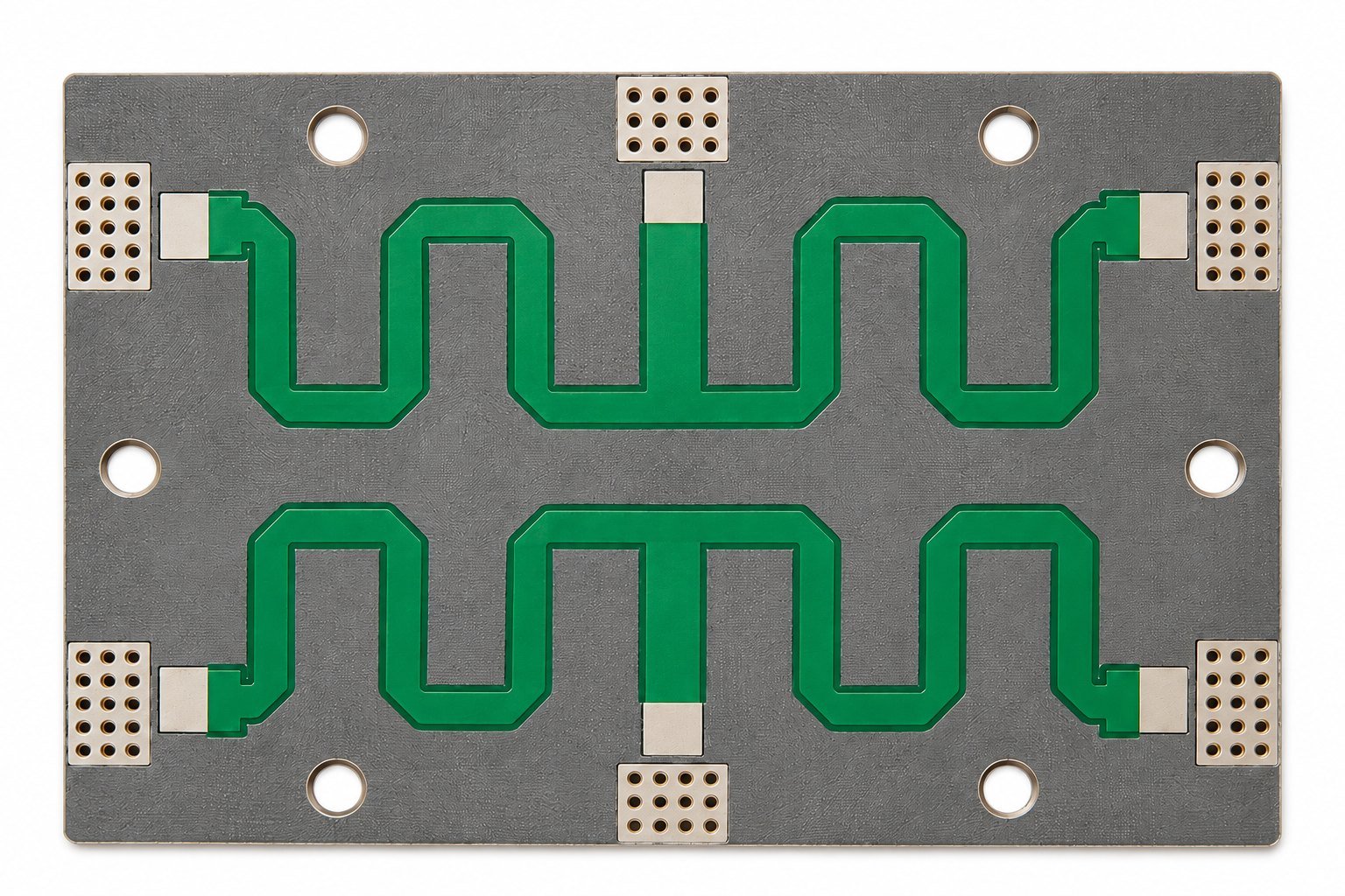
PTFE is the dielectric platform behind many demanding RF boards.
“Teflon PCB” is widely used as an industry term for circuit boards built with PTFE-based dielectric materials. In production, these are usually engineered composites rather than unfilled PTFE: glass reinforcement, ceramic fillers or other structures are used to tune dielectric, thermal and mechanical behavior.
Compared with general-purpose FR-4, PTFE-based high-frequency laminates are selected when signal loss, phase behavior, dielectric consistency or very high operating frequency becomes the dominant design requirement. The exact material is not chosen by one number alone; Dk, dissipation factor, thickness, copper roughness, thermal expansion, reinforcement style and process compatibility all matter.
Electrical performance is only one part of the material decision.
PTFE-based laminates are available in multiple Dk ranges and reinforcement systems, allowing RF designers to balance insertion loss, circuit size, thermal behavior and fabrication needs.
Very Low Dielectric Loss
Representative reinforced PTFE laminates can reach dissipation factors below 0.001 at 10 GHz, supporting low-loss transmission lines and broadband RF structures.
Controlled Dielectric Properties
Commercial PTFE laminate families span low to high Dk values, enabling either larger low-Dk structures or compact high-Dk antennas, resonators and passive circuits.
RF-Focused Material Options
Glass-reinforced, microfiber-reinforced and ceramic-filled PTFE constructions provide different tradeoffs in isotropy, rigidity, dimensional stability and thermal conductivity.
Harsh-Environment Suitability
Selected PTFE laminates combine low moisture absorption with resistance to many common processing chemicals and are used in high-frequency systems exposed to demanding environments.
PTFE laminate options cover a much wider range than “Dk ≈ 2.1”.
The examples below come from current manufacturer data and illustrate how PTFE-based laminates are engineered for different RF design priorities.
| Material | Construction | Typical / Design Dk | Typical Df | Example Design Direction |
|---|---|---|---|---|
| Rogers RT/duroid 5880 | PTFE with random glass microfiber reinforcement | 2.20 | 0.0009 @ 10 GHz | Very low-loss broadband, antenna and microwave circuits |
| Rogers RT/duroid 5870 | PTFE with random glass microfiber reinforcement | 2.33 | 0.0012 @ 10 GHz | Low-loss RF / microwave structures requiring uniform electrical properties |
| Rogers RT/duroid 5880LZ | Filled PTFE composite | 2.00 | 0.0021 @ 10 GHz | Low-density, low-Dk high-frequency structures |
| AGC RF-35TC | Ceramic-filled PTFE with fiberglass | 3.5 ± 0.05 | 0.002 @ 10 GHz | Low-loss RF with increased thermal-management emphasis |
| AGC RF-10 | Ceramic-filled PTFE with woven fiberglass | 10.2 ± 0.3 | 0.0025 @ 10 GHz | High-Dk designs where RF circuit or antenna size reduction is valuable |
Values are representative manufacturer data, not a GlobalWellPCB material guarantee. Confirm the exact grade, thickness, copper foil and latest datasheet before design release.
Rogers data-sheet Dk and Df values use the stated 10 GHz test conditions; AGC values above are from AGC Solutions Guide, June 2026, page 3. Source links identify the material data, not an approved production stackup. Sources checked 14 October 2026.
Use PTFE where RF performance needs it — not automatically on every layer.
Material cost, rigidity, bonding systems, via reliability and RF performance should be considered together when selecting a stackup.
Double-Sided PTFE PCB
Suitable for microstrip, antenna, filter and microwave circuits where the signal geometry can be implemented on a simple two-layer construction.
Multilayer PTFE Construction
Used when RF routing, shielding, grounds and interconnect density require additional layers. Bonding films and registration become critical process variables.
Hybrid PTFE / FR-4
Places the high-frequency material in RF-critical layers while other layers support power, digital routing and mechanical needs. Compatibility must be reviewed before release.
Processing reference: Rogers RT/duroid 5870–5880 fabrication guidelines. Use the processing guide for the selected grade; these instructions must not be generalized to every PTFE composite.
PTFE boards cannot be treated as ordinary FR-4 builds.
Manufacturer processing guides emphasize controlled handling, drilling, bonding and PTH preparation because PTFE-based composites can be softer, more damage-sensitive or more abrasive than standard rigid laminates.
Support Thin Cores
PTFE-based cores can be softer and easier to crease or distort. Flat support, clean work surfaces and controlled handling reduce dimensional damage before lamination.
Control Tool Condition
Fresh drills, supportive entry / exit materials and controlled feed, speed and retract parameters help maintain plated-through-hole quality in filled PTFE composites.
Prepare PTFE for Metallization
PTFE surfaces may require specialized chemical or plasma treatment before metal deposition so the surface becomes suitable for reliable PTH processing.
Match Bonding Systems
Multilayer and hybrid constructions require compatible bonding films or prepregs plus a controlled bond cycle matched to the selected material set.
Protect Critical Dimensions
Trace width, dielectric thickness and copper profile all influence impedance and insertion loss. Artwork compensation and etch control must match the RF design intent.
Confirm the Finished Build
Final checks can include dimensional inspection, electrical test and controlled-impedance coupons or measurements when specified by the project.
High-frequency systems where dielectric loss and repeatability matter.
Material choice depends on the circuit architecture, but PTFE laminates are widely represented across antenna, communication, radar and microwave passive-component applications.
Phased Arrays & RF Antennas
Low-loss laminates support feed networks, radiating elements and RF structures where phase and geometry consistency are critical.
Automotive & Aerospace Radar
High-frequency materials are used in radar front ends and antenna structures that operate at microwave and millimeter-wave frequencies.
Base Stations & Microwave Links
PTFE materials can support RF paths, filters, couplers and transmission networks in communication infrastructure.
Satellite Communications
Low-loss and stable dielectric platforms are used in satellite communication circuits where link efficiency and repeatable RF behavior matter.
Filters, Couplers & Dividers
Controlled Dk and low loss enable transmission-line structures that depend directly on substrate electrical properties.
Amplifier & Thermal Designs
Thermally enhanced ceramic-filled PTFE laminates can be selected when heat spreading and RF loss need to be managed together.
PTFE PCB construction and RF design details.
Review the selected laminate, stackup and fabrication details against your RF design requirements.
Send the stackup and RF requirements, not just the Gerbers.
PTFE quoting is more accurate when the laminate grade, dielectric thickness, copper type, impedance targets and test requirements are defined from the start.
Gerber or ODB++, NC drill files, board outline and quantity.
Exact PTFE / filled-PTFE grade, thickness and acceptable alternates.
Target impedance, controlled lines, frequency range and coupon requirements.
Copper weight / profile, surface finish, tolerances and critical dimensions.
Questions engineers ask before selecting PTFE.
Is a Teflon PCB the same as a PTFE PCB?
In PCB industry usage, “Teflon PCB” is commonly used to describe PTFE-based circuit boards. The actual laminate is usually an engineered PTFE composite with glass, ceramic or other reinforcement rather than a sheet of unfilled PTFE.
Does every PTFE PCB have a dielectric constant around 2.1?
No. Low-Dk PTFE products exist around 2.0–2.3, but ceramic-filled PTFE families can be engineered for substantially higher Dk. The right value depends on impedance, circuit dimensions, antenna size, bandwidth and other design goals.
Why is PTFE PCB fabrication more specialized than FR-4?
PTFE-based materials can require different handling, drilling, lamination and plated-through-hole surface preparation. Manufacturer fabrication guides specifically address issues such as material softness, tool wear and making PTFE surfaces suitable for metal deposition.
Can PTFE be combined with FR-4 in one multilayer PCB?
Yes, hybrid constructions are possible and are often considered when only part of the board needs a high-frequency dielectric. The complete stackup still requires engineering review for bonding compatibility, registration, thickness, thermal behavior and via reliability.
Which surface finish is best for a Teflon RF PCB?
There is no universal best finish. Selection should consider solderability, flatness, contact or wire-bond needs, RF conductor-loss sensitivity and the assembly process. Define the finish together with the frequency and interconnect requirements.
What information should be included in a PTFE PCB RFQ?
Include the exact laminate or approved material family, layer stackup, dielectric thicknesses, copper requirements, controlled impedance values, frequency-sensitive geometry, via construction, surface finish, tolerances, quantity and inspection or test requirements.