Nelco PCB Manufacturing for High-Speed, Low-Loss Designs.
Build multilayer boards around the exact Nelco material called out in your stackup. We review laminate grade, dielectric construction, controlled impedance and thermal requirements before production.
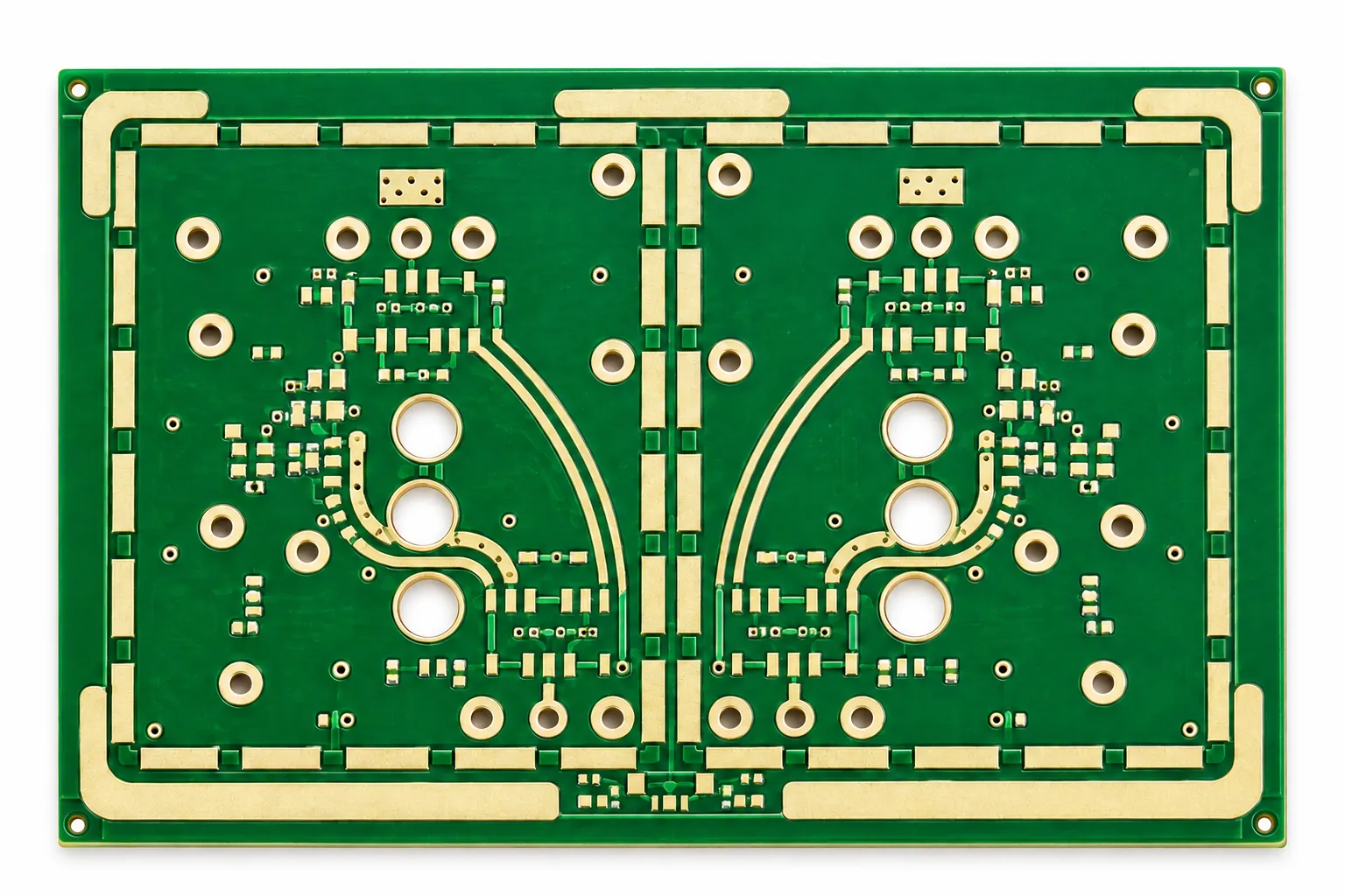
What Is a Nelco PCB?
A Nelco PCB is a printed circuit board built with a Nelco-designated laminate and prepreg system, commonly selected for high-speed digital, controlled-impedance and thermally demanding multilayer applications.
Current AGC Multi Material listings include N4000-13 family products and N7000 polyimide materials. The important design rule is simple: preserve the exact material suffix, construction and dielectric basis specified by the design instead of treating “Nelco” as a single generic laminate.
Low-loss modified epoxy options support high-speed channels, backplanes and switching platforms.
SI variants are intended for applications where electrical consistency and thickness control matter.
Selected N4000 systems are positioned for thermally demanding multilayer assembly profiles.
Material selection can support long-term reliability in dense, high-reliability interconnect structures.
Electrical Performance Without Treating the PCB as Generic FR-4.
Nelco grades are selected when the dielectric system is part of the signal, thermal or reliability design—not just mechanical support.
Lower Channel Loss
N4000-13 family materials are positioned as mid-loss modified epoxy systems for high-speed multilayer designs.
Controlled Electrical Geometry
Material Dk, pressed dielectric thickness and copper profile can be coordinated with trace geometry for impedance targets.
High-Tg Options
High-Tg and polyimide grades provide additional thermal margin for demanding fabrication and assembly environments.
CAF + Via Reliability Focus
Material choice, hole architecture and thermal excursions should be reviewed together for dense multilayer boards.
Multilayer-Friendly Processing
N4000 systems are designed for advanced multilayer PCB fabrication while maintaining project-specific process controls.
Specification Discipline
The exact Nelco grade, prepreg and core construction should remain tied to the released stackup and approved material list.
Common Nelco Material Options.
Use these values for initial material screening only. Final impedance and loss calculations should use the exact AGC data for the selected construction, resin content, test method and frequency.
Review a Specific Stackup →| Material | Resin System | Typical Dk @ 10 GHz | Typical Df @ 10 GHz | Tg | Typical Use |
|---|---|---|---|---|---|
| N4000-13 | Modified epoxy | 3.6 | 0.009 | 240°C (DMA) | High-speed storage, switching/routing, wireless infrastructure, backplanes |
| N4000-13 SI | Modified epoxy + SI glass | 3.2 | 0.008 | 240°C (DMA) | Signal-integrity and controlled-impedance multilayers |
| N4000-13 EP | Modified epoxy | 3.6 | 0.009 | 240°C (DMA) | Lead-free, high-speed multilayer applications requiring the EP grade |
| N4000-13 EP SI | Modified epoxy + SI glass | 3.2 | 0.008 | 240°C (DMA) | High-speed designs requiring EP thermal performance plus SI electrical control |
| N7000-2 HT / N7000-3 | Polyimide | 3.5 | 0.009 | 260°C (DSC) | High-reliability and severe thermal multilayer applications |
Source: AGC Solutions Guide, June 2026, page 4. Dk/Df are listed at 10 GHz. The N4000 Tg values use DMA; N7000 uses DSC. These methods are not interchangeable. Source checked 14 October 2026.
Nelco PCB Performance Starts with the Stackup.
The material family name alone is not enough to define a manufacturable or simulation-ready stackup. The released construction should identify the exact laminate/prepreg grade and the dielectric geometry used to reach the required impedance and insertion-loss targets.
- Preserve the full grade: N4000-13, N4000-13 SI, N4000-13 EP and N4000-13 EP SI should remain distinct in procurement and engineering records.
- Match Dk to the model: use the value and method appropriate to the selected glass style, resin content and operating frequency.
- Control dielectric thickness: pressed prepreg thickness and copper profile influence finished impedance.
- Review copper roughness: conductor profile can become a meaningful contributor to loss at higher data rates.
Treat Material, Drilling, Lamination and Assembly as One System.
High-speed multilayer reliability depends on more than laminate selection. Via structure, resin fill, copper distribution, lamination cycle and final assembly temperatures all interact with the material system.
- Material identity: confirm laminate and prepreg part numbers before fabrication release.
- Hybrid stackups: document interfaces and bonding requirements when combining Nelco with other RF or digital materials.
- HDI and via structures: review aspect ratio, sequential lamination and via-in-pad requirements against the complete build.
- Reflow exposure: confirm the assembly profile against the exact material grade and PCB construction.
- Coupon strategy: define impedance verification and other project-specific acceptance evidence before production.
Where Nelco PCB Materials Are Commonly Considered.
Material selection should follow the actual loss budget, impedance requirements, thermal exposure and approved material list for the project.
Backplanes & Chassis Interconnects
Dense multilayers where insertion loss, impedance and plated-hole reliability are tightly controlled.
Switching & Routing Systems
High-speed digital channels that need controlled dielectric behavior and repeatable impedance.
Wireless Infrastructure
Mixed digital and RF-adjacent systems where signal integrity, thermal reliability and stackup discipline matter.
High-Speed Storage
Server and storage interconnects with defined loss budgets, connector launches and impedance targets.
Thermally Demanding Multilayers
Designs where high-Tg modified epoxy or polyimide is chosen to support the required thermal environment.
Controlled-Impedance Designs
Multilayer channels where exact dielectric construction is part of the electrical design and verification plan.
From Material Callout to Finished Nelco PCB.
We align the material identity, stackup and quality scope before the build moves forward.
Share the Released Data
Send Gerber or ODB++, drill data, layer count, target thickness, copper, material callout and impedance requirements.
Review the Stackup
Confirm the exact Nelco grade, dielectric construction, controlled features and any hybrid-material interfaces.
Confirm Build & Evidence
Agree fabrication details, coupon requirements, inspection scope and any assembly-related thermal constraints.
Produce, Verify & Deliver
Complete the agreed checks and provide the finished boards with project-defined documentation.
What We Check Before Quoting a Nelco PCB.
Nelco projects are most reliable when the quotation is based on the full construction rather than a material name alone.
Exact Grade & Availability
Laminate/prepreg identity, suffix, construction and source route.
Dielectric & Copper Build
Layer sequence, pressed thickness, copper weights and applicable foil profile.
Impedance Requirements
Target impedance, tolerance, geometry assumptions and coupon expectations.
Via Architecture
Through, blind/buried or microvia structures and any via-in-pad requirements.
Surface Finish & Fabrication Notes
Finish, mask, edge features, tolerances and controlled mechanical requirements.
Inspection & Test Scope
Electrical test, impedance verification and project-defined documentation.
Nelco PCB FAQ.
Are N4000-13 and N4000-13 SI the same material?
No. They are related members of the N4000-13 family, but current AGC listings show different typical Dk/Df values and the SI version uses SI glass for applications requiring tighter signal-integrity performance. Keep the exact suffix in the released stackup.
Can I replace Nelco with another low-loss laminate?
Not automatically. A substitute can change dielectric behavior, pressed thickness, copper interaction, processing and reliability. Any alternative should be reviewed against the electrical model, stackup, qualification requirements and approved material list.
What Dk should be used for impedance calculations?
Use the value appropriate to the exact Nelco grade, laminate/prepreg construction, resin content, test method and operating frequency. A single headline Dk is useful for screening but is not enough for a production stackup.
Is Nelco only for RF boards?
No. Current N4000 family applications include high-speed storage, internet switching/routing, wireless infrastructure and backplanes. The family is often used for high-speed digital and controlled-impedance multilayer designs.
What files should I send for a Nelco PCB quote?
Provide Gerber or ODB++, drill data, fabrication drawing, stackup, exact Nelco material callout, copper weights, finished thickness, impedance requirements, quantity and delivery target. Add any approved-material or verification requirements that apply.
Can Nelco be used in a hybrid stackup?
Potentially, but hybrid constructions should be reviewed as a complete system. Confirm compatible bonding materials, lamination conditions, dielectric assumptions, copper construction and the electrical behavior at every material interface.