GlobalWellPCBPCB & PCBA Manufacturing
GlobalWellPCB

Megtron PCB Manufacturing for High-Speed, Low-Loss Designs

Build multilayer PCBs around Panasonic MEGTRON materials when signal integrity, transmission loss and thermal reliability are critical. We review the specified material grade, stack-up, impedance, copper profile and fabrication requirements as one engineering package.
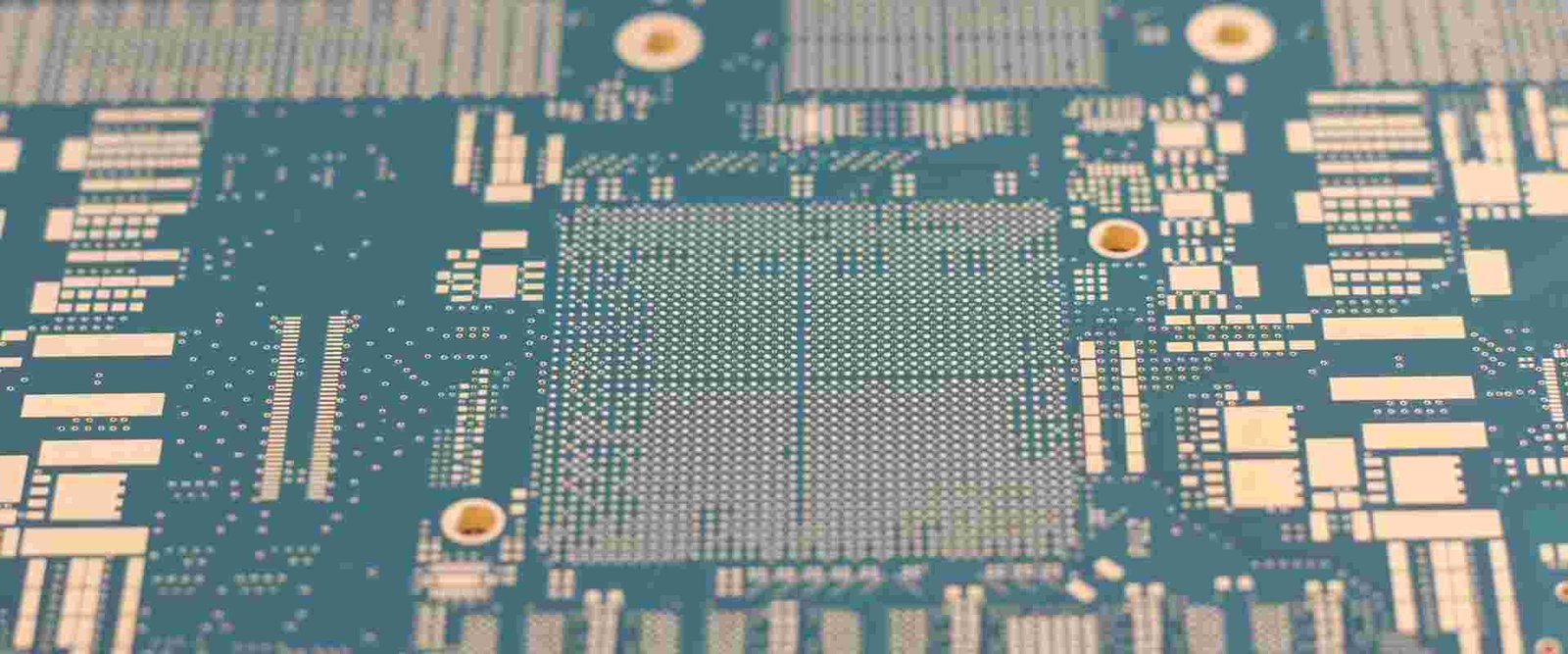
MEGTRON 6 / 7 / 8High-Layer-Count PCBControlled ImpedanceHigh-Speed Networking
01
Low-Loss Material ReviewGrade, prepreg, copper and glass style
02
Stack-Up EngineeringImpedance and dielectric construction aligned
03
High-Layer-Count BuildsThermal and registration risks reviewed
04
Project-Specific VerificationMaterial values and tolerances confirmed before build
Material Overview

What Is a Megtron PCB?

A Megtron PCB is a printed circuit board fabricated with Panasonic Industry's MEGTRON family of high-performance circuit board materials. The family is intended for lead-free, high-layer-count and other performance-sensitive boards, with a dielectric system and smooth copper options designed to reduce transmission loss.

MEGTRON is not a single laminate. Different series and grade variants target different levels of loss, thermal performance and high-speed requirements. For that reason, a purchase specification should identify the exact laminate/prepreg grade instead of only stating “Megtron.”
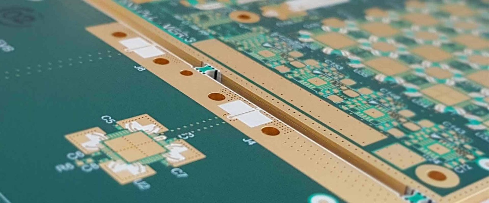
Important: MEGTRON is a Panasonic material brand. GlobalWellPCB is not presented here as the material manufacturer. Final material selection and availability should be confirmed against the current Panasonic datasheet and the approved production stack-up.
Why Engineers Specify It

Where Megtron Adds Value.

The material decision matters most when insertion loss, high-frequency consistency and multilayer reliability become part of the electrical design.

01 / SIGNAL

Low Transmission Loss

Low Df and smooth-copper constructions help reduce conductor and dielectric losses in long, fast channels.

02 / THERMAL

High Heat Resistance

MEGTRON 6, 7 and 8 are positioned as highly heat-resistant multilayer materials for demanding fabrication and assembly conditions.

03 / DENSITY

High-Layer-Count & HDI

Selected MEGTRON families support dense interconnect structures and high layer counts used in advanced networking platforms.

04 / SYSTEM

Designed for High-Speed Platforms

Typical use cases include routers, switches, servers, optical transmission equipment and other data-intensive electronics.

Series Selection

MEGTRON 6 vs. MEGTRON 7 vs. MEGTRON 8.

Do not choose by series number alone. Use the specified grade, tested frequency, copper profile and complete stack-up to make the engineering decision.

ESTABLISHED ULTRA-LOW-LOSS PLATFORM

MEGTRON 6

Widely used in ICT infrastructure and other high-speed designs. Panasonic describes it as an industry-standard high-speed, ultra-low-loss PCB material with strong HDI and thermal performance.

  • Example laminateR-5775(N)
  • Example prepregR-5670(N)
  • Typical Dk3.34 @ 13 GHz
  • Typical Df0.0037 @ 13 GHz
LOWER-LOSS / HIGH-DATA-RATE

MEGTRON 7

Targeted at high-speed, large-data-volume equipment such as servers and routers. Panasonic highlights ultra-low Dk/Df and compatibility with very high layer counts and HDI layouts.

  • Example laminateR-5785(N)
  • Example prepregR-5680(N)
  • Typical Dk3.31 @ 14 GHz
  • Typical Df0.0023 @ 14 GHz
NEXT-GENERATION NETWORKING

MEGTRON 8

Developed for next-generation high-speed communication network equipment. Panasonic positions the family for 800GbE. Its published comparison reports about 30% lower transmission loss at 28 GHz for MEGTRON8 R-579Y(U) / R-5795(U) versus MEGTRON7 R-578Y(N) / R-5785(N); this is a manufacturer material comparison, not a guaranteed improvement for a finished PCB. See Panasonic's comparison and conditions.

  • Example gradeR-579Y(U) / R-569Y(U)
  • Typical Dk3.08 @ 14 GHz
  • Typical Df0.0012 @ 14 GHz
  • Tg (DMA)220°C
Reference Data

Typical Material Properties for Design Discussion.

Use these values only as a quick comparison. Exact values depend on grade and test method.

Series / Example GradeDkDfTgTdWater AbsorptionTypical Positioning
MEGTRON 6
R-5775(N) / R-5670(N)
3.34 @ 13 GHz0.0037 @ 13 GHz185°C DSC
210°C DMA
410°C0.14%High-speed ICT, networking, measurement equipment, antenna-related applications
MEGTRON 7
R-5785(N) / R-5680(N)
3.31 @ 14 GHz0.0023 @ 14 GHz200°C DSC
210°C DMA
400°C0.06%Servers, routers, 5G-related high-speed and large-data-volume platforms
MEGTRON 8
R-579Y(U) / R-569Y(U)
3.08 @ 14 GHz0.0012 @ 14 GHz220°C DMA370°C0.06%800GbE and next-generation high-speed networking equipment

Typical values above are summarized from Panasonic Industry public product information and are not guaranteed production values. Dk/Df cannot be compared responsibly without considering frequency, test method, resin content, glass style and copper roughness. Verify the latest official datasheet for the exact part number used on your PCB.

Electrical test conditions: MEGTRON6 uses 13 GHz (April 2022 sheet); MEGTRON7 uses 14 GHz (July 2024 sheet); MEGTRON8 uses 14 GHz. Panasonic specifies balanced-type circular disk resonance, C-24/23/50, on a 0.75 mm sample. These typical values depend on the glass, resin and copper construction. Sources checked 14 October 2026.

DFM & Stack-Up

Megtron PCB Design Needs More Than a Material Name.

For high-speed boards, the laminate is only one part of the channel. Resin content, woven-glass construction, copper foil profile, dielectric thickness and trace geometry all influence impedance and insertion loss.

01 / GRADE

Specify the Exact Part Number

State laminate and prepreg grades where the design has been qualified around a specific construction.

02 / IMPEDANCE

Provide Controlled-Impedance Targets

Include target impedance, tolerance, referenced layers and coupon/test requirements.

03 / COPPER

Control Copper Profile

Low-profile or very-low-profile copper can materially affect high-frequency conductor loss and should not be treated as interchangeable.

04 / GLASS

Review Glass Style & Resin Content

Actual dielectric behavior is construction dependent. Core and prepreg choices should be reviewed with the final stack-up.

05 / VIAS

Plan Via Structures Early

High-layer-count and HDI designs require coordinated decisions on aspect ratio, sequential lamination and reliability.

06 / LOSS BUDGET

Connect PCB Data to the Channel Budget

For critical links, review material loss assumptions together with routing length, connector loss and the required signaling architecture.

Manufacturing Control

Focus the Build Around What Changes Electrical Performance.

For low-loss multilayer PCBs, material traceability, stack-up control and finished-board verification deserve explicit acceptance criteria.

Material identity, incoming documentation and approved substitutions.
Registration, dielectric thickness and via/plating structure verification.
Project-defined impedance coupon and finished-board electrical checks.
Applications

Where Megtron PCB Materials Are Commonly Evaluated.

Compare applications by their electrical, thermal and construction requirements, then select the exact MEGTRON grade for your design.

AI Servers & Data Centers

High-speed backplanes, accelerator platforms and dense server interconnects with demanding channel budgets.

Routers & Switches

High-capacity network equipment where insertion loss and dense multilayer routing directly affect link performance.

5G & Telecom Infrastructure

Wireless and transport equipment requiring low-loss multilayer interconnects and stable high-frequency behavior.

Test & Measurement

Semiconductor test equipment, probe-card-related systems and precision high-speed instrumentation.

Project Workflow

From Material Callout to Production Stack-Up.

Lock the electrical assumptions before committing the multilayer build.

Share Design Data

Provide Gerber or ODB++, drill data, stack-up, material callout, quantity and controlled-impedance requirements.

Review Material & Stack-Up

Confirm the exact MEGTRON grade, construction, copper profile and any approved alternates before quoting the final build.

Approve Engineering Questions

Resolve DFM items, impedance structures, via architecture and tolerances against the controlled production data set.

Fabricate & Verify

Build to the approved stack-up and complete the agreed inspection, electrical and impedance verification scope.

Start a Megtron PCB RFQ

Send the Stack-Up, Not Just the Board Outline.

For high-speed Megtron designs, complete technical inputs reduce back-and-forth and make the quotation more meaningful.

Fabrication Data

Gerber/ODB++, drill files, board dimensions, layer count and quantity.

Material Specification

Exact MEGTRON laminate/prepreg grade, or the approved electrical requirements if alternatives may be reviewed.

Electrical Controls

Impedance targets/tolerances, reference layers, differential pairs and any insertion-loss or test-coupon requirements.

Construction Details

Copper weights, finished thickness, via structures, surface finish and any reliability/test requirements.

Common Questions

Megtron PCB FAQ.

Is MEGTRON a single PCB material?

No. MEGTRON is a family of Panasonic circuit board materials. Different series and grade variants have different dielectric, thermal and processing characteristics, so the exact laminate/prepreg part number should be identified for controlled designs.

What is the difference between MEGTRON 6, 7 and 8?

In broad terms, the later high-performance families target progressively lower transmission loss and higher-speed networking requirements. For example, Panasonic lists MEGTRON 7 R-5785(N) at a typical Df of 0.002 at 12 GHz, while MEGTRON 8 R-579Y(U) is listed at 0.0012 at 14 GHz. Test frequency and method differ, so values should not be compared without context.

Can FR-4 be substituted for Megtron?

Not automatically. If the design was qualified around Megtron's loss, thermal or dimensional behavior, switching to conventional FR-4 can change impedance and channel loss. Any substitution should be evaluated against the electrical and reliability requirements.

Why does copper roughness matter on a Megtron PCB?

At high frequency, current is concentrated near conductor surfaces. Rougher copper increases effective path length and conductor loss, which can reduce the benefit of selecting a low-loss dielectric. Copper profile should therefore be part of the stack-up discussion.

What files are needed for a Megtron PCB quotation?

Provide fabrication data, drill files, layer stack-up, exact material callout, copper requirements, finished thickness, impedance targets, surface finish, quantity and any special inspection/test requirements. For high-speed projects, include the electrical constraints that drove the material selection.

Does specifying “MEGTRON 7” fully define the material?

No. MEGTRON 7 includes multiple grade variants. The laminate and prepreg part number, glass/resin construction and copper profile can matter to the final electrical result. Use the complete approved material specification whenever possible.

Technical references: Panasonic Industry public MEGTRON Series, MEGTRON 6, MEGTRON 7 and MEGTRON 8 product information and datasheets; application/context cross-checked against Panasonic public networking/5G materials. Panasonic and MEGTRON are trademarks of their respective owner. Refer to Panasonic's current datasheets for material specifications. Typical material data must be verified against the latest official datasheet and the actual approved PCB construction before release.

Scroll to Top