GlobalWellPCBPCB & PCBA Manufacturing
RF & Microwave PCB

RF PCB Manufacturing

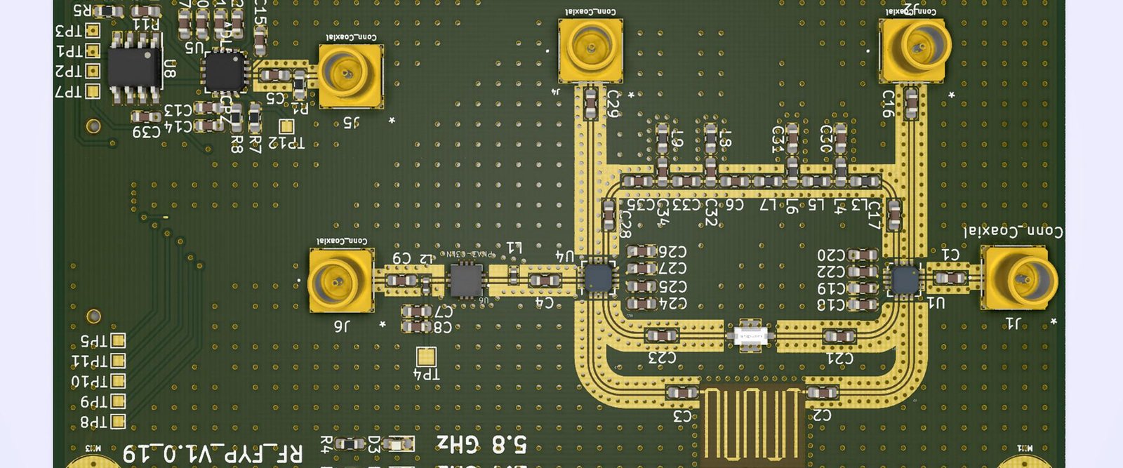
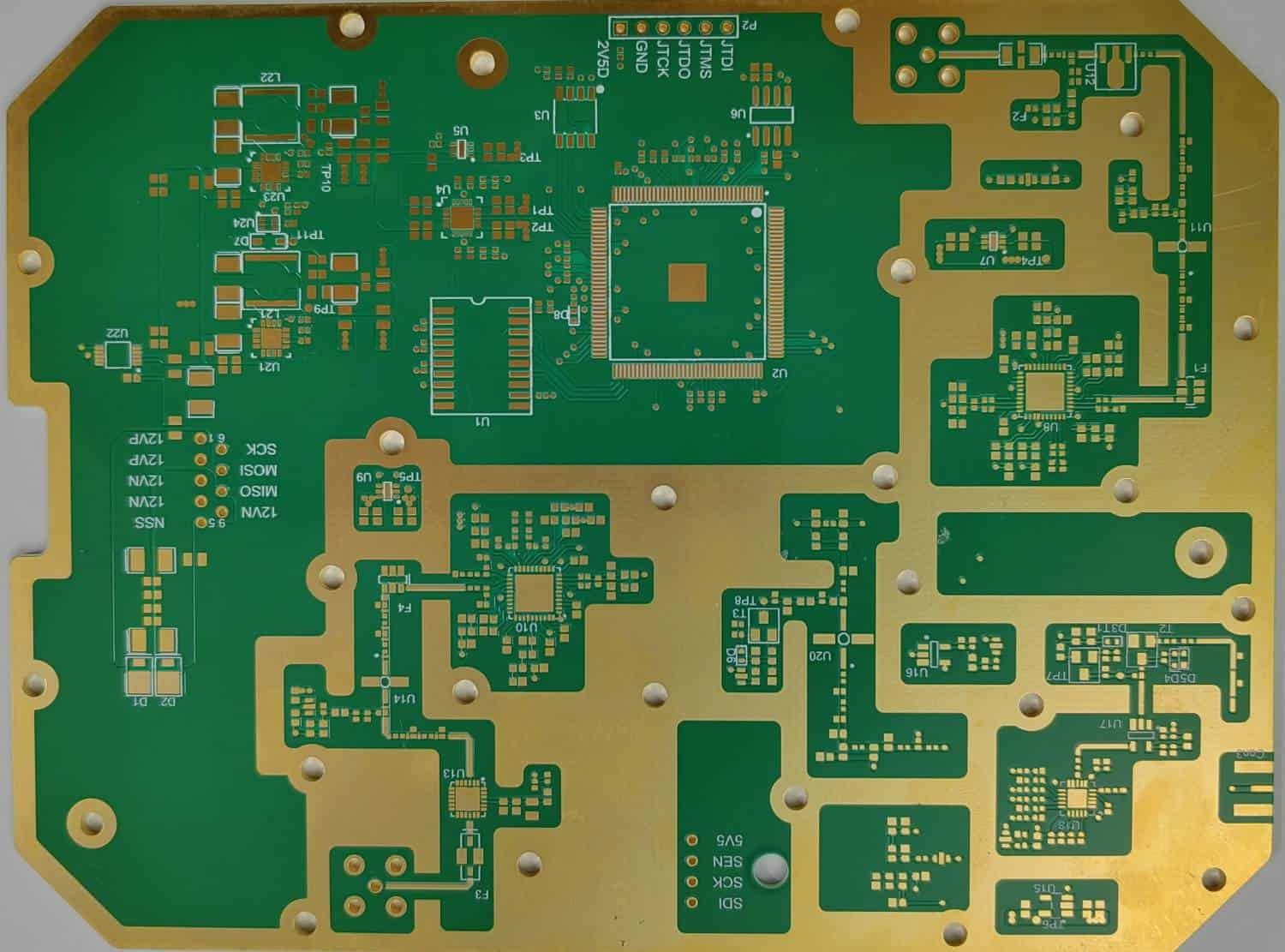
High-frequency PCB fabrication built around your signal path, laminate choice, stackup and controlled-impedance requirements. From Rogers-based and PTFE constructions to hybrid RF/FR-4 builds, each project is reviewed against the actual operating requirements.
01
Material ReviewRogers, PTFE & hybrid constructions
02
Controlled GeometryImpedance, reference planes & transitions
03
Project ValidationInspection and RF test scope defined up front
01 / RF PCB Essentials

What makes an RF PCB different?

An RF PCB uses PCB traces and reference conductors as controlled transmission structures. At high frequencies, trace geometry, dielectric properties, copper characteristics, ground continuity and transitions can materially affect signal integrity.

That means the board cannot be evaluated from the schematic alone. The laminate, copper, finished dielectric thickness, line structure, stackup and manufacturing tolerances need to be considered together.

RF PCB is an application category, not a material brand. Rogers is one supplier of high-frequency laminates. An RF PCB may use Rogers materials, PTFE-based materials, other low-loss laminates or, where the design permits, selected FR-4 constructions.
02 / RF PCB Applications

Common RF and microwave board applications.

Explore RF PCB requirements for antenna, radar, amplifier, 5G and microwave designs, including signal loss, material selection and controlled impedance.

01 / ANTENNA

Antenna & Feed Networks

Boards where feed geometry, reference planes, launch design and phase consistency are part of RF performance.

02 / RADAR

Radar & Sensing

RF and microwave circuits requiring stable dielectric properties and tightly controlled signal-path geometry.

03 / AMPLIFIER

RF Power & Amplifier Boards

High-frequency layouts where impedance matching, grounding and thermal behavior need to be reviewed together.

04 / WIRELESS

5G & Wireless Infrastructure

Radio, transceiver and network hardware with low-loss routing and controlled transitions across the RF path.

05 / MICROWAVE

Microwave & Satellite

Low-loss material systems and stable stackups for microwave links, satellite communication and related systems.

06 / TEST

RF Test & Measurement

Fixture and instrumentation boards where reference planes, connector launches and repeatable transmission paths matter.

03 / RF PCB Materials

Select the laminate, then define the full stackup.

Material data below is based on current Rogers published values. Final selection must match the circuit, thickness, copper and fabrication route.

Compare RF material examples, then confirm the exact grade and availability for your order.
MaterialProcess DkDesign DkTypical DfPractical selection note
Rogers RO4003C™3.38 ± 0.053.550.0027 @ 10 GHzHydrocarbon/ceramic laminate with processing characteristics closer to common PCB fabrication than PTFE materials.
Rogers RO4350B™3.48 ± 0.053.660.0037 @ 10 GHzHydrocarbon/ceramic laminate; Rogers lists UL 94 V-0 rating for the material.
RT/duroid® 58802.20 ± 0.022.200.0009 @ 10 GHzGlass-microfiber reinforced PTFE laminate intended for very low-loss high-frequency and broadband use.
Taconic / Other RF LaminatesGrade dependentGrade dependentGrade dependentSpecify the exact manufacturer and grade. Electrical values and fabrication behavior should not be generalized by brand.
Hybrid RF + FR-4Construction dependentConstruction dependentConstruction dependentUseful when high-frequency material is needed only in selected layers; bonding compatibility and final stackup require review.

Dk and Df depend on the manufacturer’s specified test method and conditions. Use the current laminate data sheet and the value appropriate to your simulation/modeling method.
Compare additional grades in the Rogers laminate selection guide. The fabrication review on this page starts from your specified grade and electrical requirements. Manufacturer sources checked 14 October 2026.

RO4003C/RO4350B process Dk and Df are specified at 10 GHz / 23°C by clamped stripline; their design Dk uses differential phase length at 8–40 GHz. The RO4350B 4 mil process Dk is 3.33 ± 0.05, and LoPro constructions require separate confirmation. Use the exact data-sheet construction for your model.

04 / RF PCB Design Review

The signal path is part of the PCB construction.

Analog Devices’ RF layout guidance reinforces the importance of continuous ground, controlled line geometry and isolation between RF, digital and power routing.

01

Controlled transmission lines

Define microstrip, grounded coplanar waveguide, stripline or other structures together with the target impedance and tolerance.

02

Continuous reference planes

Avoid plane splits beneath critical RF routes. Return-path continuity needs to follow the signal through the stackup.

03

Ground via strategy

Ground vias can help control parasitic inductance and coupling around RF structures, launches and grounded components.

04

Connector and via transitions

Transitions can create local impedance discontinuities. Include launch geometry and layer changes in the design and validation plan.

05

RF / digital isolation

Separate high-speed digital and power-noise sources from sensitive RF paths and maintain appropriate grounding between functional regions.

06

Copper, mask and finish

Copper roughness, finished geometry, solder-mask openings and surface finish can influence the final transmission structure and loss.

RF layout background: Analog Devices — PCBs Layout Guidelines for RF & Mixed-Signal. Apply this general guidance with the component reference design and project-specific stackup; it is not a finished-board test result.

05 / RF PCB Manufacturing

Turn design intent into a controlled build package.

Send your RF board files, laminate grade, stackup and impedance targets for a quotation. Include operating frequency and signal-loss requirements so we can review the complete construction.

The goal is to lock the approved laminate, stackup, copper, impedance structures, special processing and inspection requirements before release.

Avoid silent substitutions. A change in dielectric grade or thickness can require new trace geometry and renewed validation. Any alternative material should be approved against the design requirements.

What to provide for RF PCB review

Fabrication files
Gerber or ODB++, NC drill, outline and revision-controlled fabrication notes.
Stackup & material
Exact core/prepreg or bonding grades, finished dielectric thicknesses and copper requirements.
Controlled RF nets
Target impedance, allowed tolerance, line structure and reference layers.
Critical transitions
Connector launches, RF vias, layer changes and any geometry that must remain fixed.
Acceptance criteria
Coupon, electrical test, impedance measurement and RF validation requirements.
01 / INPUT

Share project data

Identify operating requirements, files, stackup and critical RF features.

02 / REVIEW

Confirm the construction

Resolve material, copper, controlled geometry and manufacturing questions.

03 / BUILD

Release approved data

Fabricate against the agreed revision and defined inspection plan.

04 / VERIFY

Inspect & validate

Complete the project-defined electrical, impedance or RF measurements.

06 / Inspection & RF Validation

Use the right test for the question you need answered.

Electrical continuity, impedance verification and RF performance measurements are related, but they do not prove the same thing.

01

Bare-board electrical test

Checks continuity and isolation of the fabricated PCB. It does not by itself validate RF insertion loss or return loss.

02

Impedance verification

Uses the agreed structure/coupon and method to check whether the manufactured transmission line matches the specified impedance range.

03

RF performance measurement

Where required, define insertion loss, return loss or other S-parameter limits across the operating band, including fixtures and calibration reference planes.

Testing scope, fixtures, calibration, measurement limits and reporting should be confirmed in the quotation. RF measurements, fixtures and reports are included only when specified in the agreed quotation.

07 / RF PCB FAQ

Questions buyers usually need answered before quotation.

Does every RF PCB need Rogers material?

No. Material choice depends on loss, frequency, route length, stackup, thermal requirements and the acceptable design margin. Rogers materials are common options, not a universal requirement.

What is the difference between RF PCB and microwave PCB?

Both involve high-frequency transmission structures. “Microwave PCB” generally refers to designs working further into microwave frequency ranges, but practical fabrication decisions should be based on the actual operating band and performance limits rather than the label alone.

Can Rogers material be combined with FR-4?

Yes, hybrid constructions are used to place low-loss material only where needed. The full bonding system, layer sequence, thermal behavior and manufacturability still need to be reviewed before release.

Can RO4003C and RO4350B be substituted directly?

Not automatically. Their published electrical properties differ, and the material flammability ratings also differ. Any substitution should be checked against the stackup and controlled geometry before fabrication.

What should be included in an RF PCB RFQ?

Include board files, drill files, stackup, exact material grade, copper, finish, controlled-net list, impedance targets, operating band, critical RF paths, quantity and required inspection/test scope. Add BOM and placement data for PCBA.

Does impedance testing prove RF performance?

No. Impedance testing addresses characteristic impedance or discontinuities in the transmission structure. RF performance over frequency may require separate S-parameter or functional measurements with defined fixtures and reference planes.

Scroll to Top