Antenna PCB Manufacturing
Build printed antenna boards around the electrical details that matter: RF material, dielectric thickness, feed-line geometry, ground structure, controlled impedance and the antenna keep-out region.
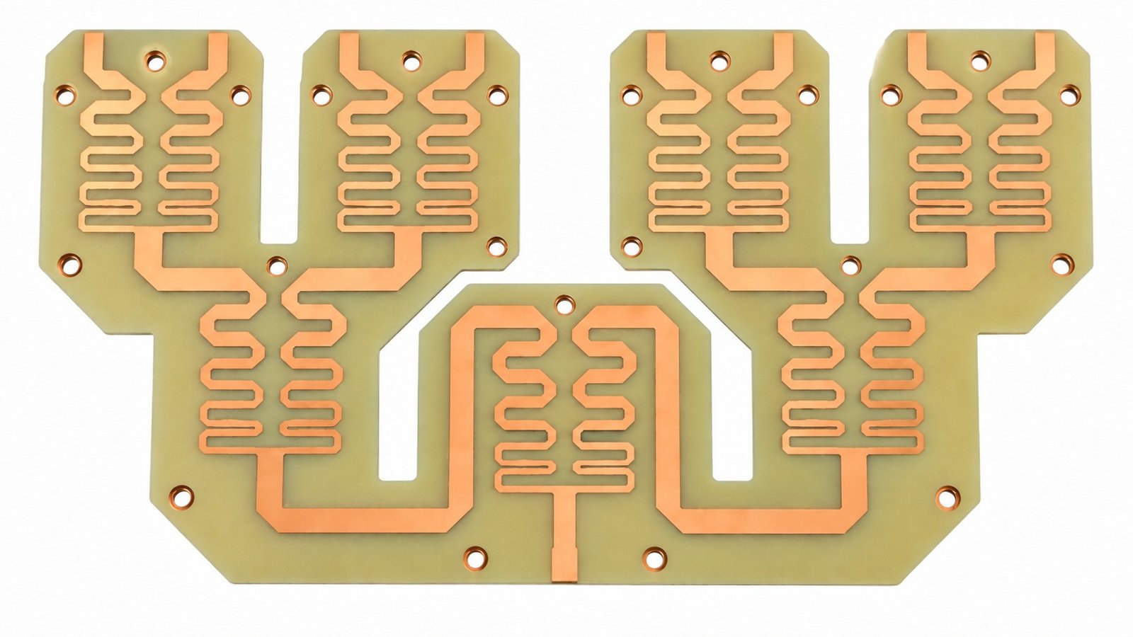
When the PCB Becomes Part of the Antenna.
A PCB antenna places the radiating structure directly on the circuit board rather than treating the antenna only as a separate external component. This approach can reduce component count and package size while allowing the RF geometry to be integrated with the rest of the product.
For manufacturing, that means the antenna artwork cannot be separated from the stackup. Material properties, conductor geometry, ground reference, feed-line impedance and nearby copper all influence the finished RF structure.
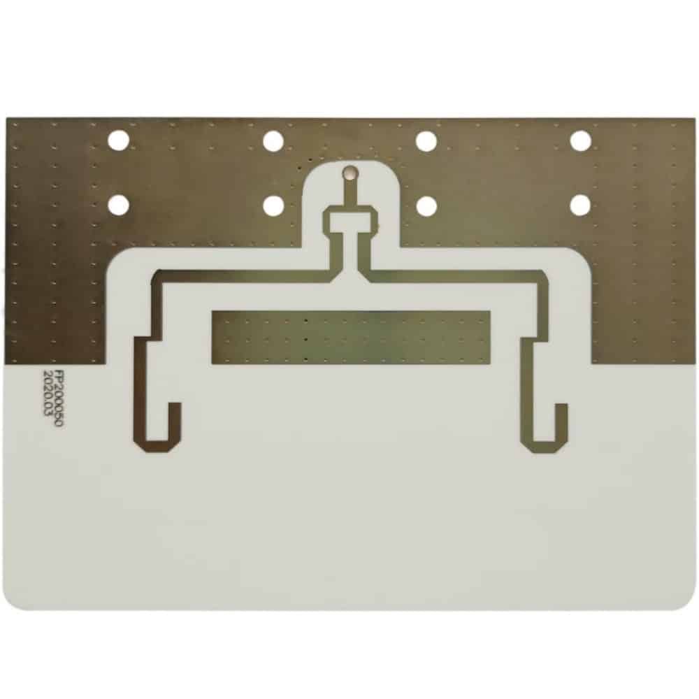
The antenna element can be formed as part of the PCB copper pattern, supporting compact product architectures.
Production files define the antenna trace or patch together with the rest of the board artwork.
Monopole, PIFA, patch, loop, slot and other structures can be selected around frequency, form factor and radiation requirements.
Cost-sensitive FR-4 constructions and lower-loss RF laminate families can be reviewed against project requirements.
PCB Antenna Types We Can Review for Manufacturability.
Antenna selection is driven by frequency, board area, radiation pattern, bandwidth, gain, enclosure and integration constraints.
Monopole & PCB Trace
Simple printed radiators commonly integrated at a board edge and designed around a defined ground reference.
PIFA / Inverted-F
Compact antenna structures often used where the layout must fit a constrained wireless product enclosure.
Patch Antenna
Low-profile printed structures using a conductive patch, dielectric substrate and ground plane.
Loop / NFC / RFID
Printed loop structures used in near-field and inductively coupled applications such as NFC and RFID.
Slot Antenna
Radiating slots formed in a conductive area, with performance tied closely to geometry and the surrounding ground structure.
Printed Dipole
A balanced two-element structure that can be integrated into wireless sensors and other compact RF products.
Meander-Line Antenna
A folded trace geometry used to increase electrical path length within a limited physical board area.
Multi-Element & Array PCB
Projects with multiple radiating elements require tighter coordination of RF geometry, isolation, feed networks and stackup.
The RF Details to Lock Before Fabrication.
At antenna frequencies, seemingly small PCB variations can become electrical variations. The manufacturing review should therefore connect the antenna artwork to the intended material system and critical dimensions.
Confirm laminate family, dielectric constant data, loss characteristics and material availability for the intended frequency and product constraints.
Core or prepreg thickness between the antenna/feed layer and its reference plane is part of the RF geometry and must be controlled as a stackup input.
Microstrip or coplanar feed geometry should be tied to the approved stackup. Target impedance and permitted tolerance should be defined in the fabrication data.
Ground-plane shape, copper clearances, edge location, shielding and nearby metal can materially affect the antenna. Keep-out requirements should be explicit.
Critical antenna trace width, gap, slot, patch dimensions and registration should be identified so they can be reviewed against the selected process.
Surface finish and solder-mask coverage can change the effective RF structure. Antenna openings and finish requirements should be shown in the manufacturing files.
Ground vias, via fences and stitching patterns around RF structures should be fabricated to the approved layout rather than altered during production.
Final antenna tuning depends on the complete device environment. Manufacturing should preserve the intended board geometry while system-level tuning remains part of product validation.
Select the Laminate Around Frequency, Loss and Geometry.
For related construction choices, review Rogers PCB materials, high-frequency PCB manufacturing, controlled-impedance requirements.
Rogers identifies high-frequency circuit materials for antenna applications including GNSS, cellular, V2X and other wireless systems. Material selection should still be project-specific.
Manufacturer sources: Rogers automotive circuit-material overview (communications antennas including GNSS, cellular and V2X) and Rogers antenna-material applications. These references describe supplier materials; availability and suitability are confirmed for your order.
| Material Family | Where It Fits | Manufacturing Review Focus |
|---|---|---|
| FR-4 / High-Tg FR-4 | Cost-sensitive RF products where the electrical requirements are compatible with the selected grade. | Dk variation, dielectric thickness, loss, copper geometry and final RF validation. |
| Rogers RO4000® Family | High-frequency antenna and RF circuits requiring tighter electrical consistency and lower loss than standard FR-4. | Approved laminate grade, thickness, copper type, bonding construction and hybrid-stackup compatibility. |
| Rogers RO3000® Family | Higher-performance RF/microwave and antenna structures, including applications where low loss and stable dielectric properties are important. | PTFE/ceramic processing, dimensional control, copper treatment and approved fabrication sequence. |
| Other RF Laminates | Taconic, Isola, Arlon or other customer-specified high-frequency materials may be considered when called out by part number. | Availability, material certificate requirements, stackup compatibility and process confirmation. |
| Hybrid RF + FR-4 | Multilayer constructions that place RF material only where the antenna/feed network needs it while retaining conventional layers elsewhere. | Bonding materials, thickness build-up, registration, drilling and lamination compatibility. |
Antenna PCBs Across Connected Products.
Printed antenna structures are used where wireless function, mechanical packaging and board integration need to be solved together.
IoT & Wireless Sensors
Compact wireless nodes using Wi-Fi, Bluetooth, sub-GHz or application-specific radio links.
GNSS / GPS Devices
Navigation, tracking and telematics products using printed patch or other integrated antenna structures.
NFC & RFID
Loop antenna PCBs for contactless identification, access, tagging and short-range coupling applications.
Wi-Fi & Bluetooth Products
Routers, controllers, gateways and embedded devices with board-level antennas or antenna feed networks.
Vehicle Connectivity
Wireless, GNSS, V2X and related antenna-board applications where RF laminate consistency may be important.
Industrial Wireless Systems
Remote monitoring, controls and communications equipment with environment- and enclosure-specific antenna constraints.
Control the PCB Features That Influence RF Performance.
Inspection should focus on the critical physical inputs defined by the antenna design and stackup.
Material Verification
Confirm the approved laminate family, thickness and construction before release.
Critical Dimensions
Inspect defined antenna traces, gaps, slots and other RF-sensitive artwork features.
Coupon-Based Control
Use controlled-impedance coupons and acceptance limits when they are part of the project requirement.
RF Validation Scope
Return loss, resonance, gain or radiation-pattern testing requires project-specific methods and is not assumed by default.
From RF Files to Production Release.
Antenna boards benefit from technical review before material purchasing and fabrication begin.
Share the RF Inputs
Send Gerber/ODB++, stackup, material grade, finished thickness, copper requirements and impedance targets.
Identify Critical Features
Mark antenna geometry, RF feed lines, controlled gaps, keep-out regions and any dimensions requiring tighter control.
Review & Confirm
Resolve material availability, stackup, tolerances, finish, solder mask and inspection scope before release.
Fabricate & Verify
Manufacture to the approved data, complete agreed inspections and provide project-defined test records where applicable.
Antenna PCB Manufacturing FAQ.
What information should be included for an antenna PCB quotation?
Include the PCB fabrication data, stackup, exact material grade where specified, dielectric and copper thicknesses, controlled-impedance targets, surface finish, solder-mask requirements, quantity and any critical RF dimensions or test requirements.
Can antenna PCBs use FR-4?
Some antenna designs can use FR-4, while others benefit from lower-loss or more tightly controlled high-frequency laminates. The decision depends on frequency, bandwidth, efficiency, dimensional constraints, cost and the design’s tolerance to material variation.
Why is the ground plane important on an antenna PCB?
For many printed antenna structures, the ground reference is part of the antenna system. Its size, shape, clearance and relationship to the feed line can change impedance and radiation behavior, so it should be treated as controlled design data.
Can you change an RF material to an equivalent grade?
Material substitutions should not be made automatically on antenna or controlled-impedance projects. Any proposed alternative should be reviewed against the electrical properties, thickness, copper system and the design’s RF requirements before approval.
Is antenna RF performance testing included with every PCB order?
No. PCB fabrication inspection, impedance verification and full antenna RF measurements are different scopes. Return loss, resonance, gain and radiation-pattern testing require defined fixtures, methods and acceptance criteria and should be agreed before quotation.
Should solder mask cover the antenna element?
That depends on the design. Solder mask changes the dielectric environment above the copper, so the antenna designer should define whether the radiating element and RF feed areas require solder-mask openings.