Glass PCB Materials and Manufacturing Review
Explore glass PCB options for designs with optical, electrical or through-glass interconnect requirements. Send your substrate, conductor and via specifications to discuss a suitable manufacturing route.
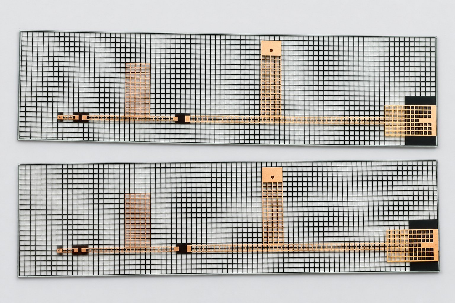
What Is Glass PCB?
A glass PCB uses a solid glass substrate carrying patterned conductors. It is different from glass-fiber-reinforced FR-4.
When to Use It?
Consider the material when the design needs an optical path, specified dimensional behavior or measured dielectric properties that justify a specialist process.
Key Constraint?
Brittleness, conductor adhesion, via formation, assembly interfaces and thermal limits must be reviewed for the actual construction.
What Is a Glass PCB and When Is It Considered?
A glass substrate PCB uses a solid glass sheet or wafer rather than a resin laminate reinforced with woven glass. The metallization and patterning route must suit the selected substrate.
Glass grades differ in thermal expansion, dielectric behavior and transmission. Borosilicate and fused silica are glass options; crystalline quartz is not interchangeable with fused silica, and sapphire is a crystalline ceramic rather than glass.
A transparent PCB requirement should define wavelength and clear aperture, not just a clear base. Review brittleness, conductor adhesion, TGV feasibility and assembly stress before assigning production limits, pricing or delivery dates.
Borosilicate, Fused Silica and Transparent Substrate Alternatives
Choose the exact grade first. Values for one borosilicate glass do not characterize every glass PCB, and substrate heat resistance is not a finished-board operating rating.
Soda-Lime Glass
Evaluate for applications where the optical, chemical and thermal requirements fit the selected grade. Confirm conductor adhesion and handling before committing to a circuit process.
Borosilicate Glass
BOROFLOAT 33 is one published material example. SCHOTT lists a CTE of 3.25 ppm/K over 20–300°C; this does not establish a complete PCB temperature rating.
Fused Silica
A glass alternative to review for optical and dimensional requirements. Fused silica is amorphous; crystalline quartz must be specified separately rather than treated as the same substrate.
Sapphire — Not Glass
Sapphire is single-crystal alumina. It can be evaluated as a transparent ceramic alternative, but is not a glass PCB material and requires its own metallization and assembly review.
Material references: SCHOTT glass data and Kyocera sapphire classification. Published material examples are not a stock list or GlobalWellPCB capability guarantee.
Glass PCB Manufacturing Requirements to Confirm
Review these parameters before assigning manufacturing limits. No universal trace width, via size, panel size or lead time applies across all glass circuit processes.
| Parameter | What to specify | What requires confirmation |
|---|---|---|
| Glass grade | Manufacturer designation, thickness and surface requirements | Procurement, flatness, handling and process compatibility |
| Circuit geometry | Minimum line, space and pad dimensions | Patterning route and conductor thickness |
| Metallization | Seed, adhesion and conductor system | Adhesion evidence, patterning and finishing |
| TGVs / holes | Via diameter definition, depth and layer connections | Formation method, aspect ratio and metallization |
| Board outline | Dimensions, edge condition and support features | Panel utilization, singulation and mounting |
| Optical window | Wavelength, transmission and clear aperture | Loss from conductor, mask, coatings and assembly |
| Surface finish | Soldering, bonding and storage conditions | Compatible finish and acceptance criteria |
| Schedule and quantity | Prototype or production quantity and requested date | Reviewed process route, availability and quotation |
On smaller screens, scroll this table horizontally to compare all columns.
Trace Design Guidelines and Best Practices
Glass PCB design must account for substrate brittleness, thermal mismatch, copper adhesion and assembly constraints.
Trace Geometry
Agree line width, spacing and pad geometry with the chosen conductor process. Do not carry over an unverified FR-4 rule set.
Clearance and Isolation
Specify working voltage and electrical clearances. Fabrication spacing and application insulation requirements are separate checks.
Conductor Transitions
Review abrupt geometry changes, pad entries and stress-sensitive features for the actual metallization system.
Pad and Joint Design
Coordinate pad geometry, adhesion requirements and component attachment with the expected thermal cycling.
Via Formation Method
TGV formation may use laser-based processing or suitable photo-structuring and etching. Select a qualified route for the glass grade.
Edges and Mounting
Specify edge finish, cutouts, support and allowable clamping loads. Avoid unreviewed stress concentrators.
Optical Alignment
Specify fiducials and alignment contrast suitable for a transparent substrate and the assembly equipment.
Conductor Thickness
Select thickness from electrical load, patterning capability, adhesion and stress, not a universal copper range.
Photo-structuring and etching are documented for suitable glass systems; see SCHOTT FOTURAN II. “Laser drilling only” is not a universal rule for glass substrates.
Glass PCB Manufacturing Process Overview
The workflow depends on the glass and conductor system. This is a planning sequence rather than a fixed process recipe; via formation and metallization must be coordinated.
Substrate Review
Approve the glass grade, thickness, optical requirements and incoming inspection.
Form Holes and Features
Create qualified vias, openings and outline features at the appropriate process stage.
Clean and Prepare
Clean and condition the surface for the approved adhesion and seed system.
Define Circuit Pattern
Use the imaging and patterning method selected for the required feature geometry.
Build Conductors
Complete the agreed deposition, plating or etching route, including via metallization where required.
Apply Protection
Add compatible solder mask or protective coating only where needed; keep optical windows clear.
Finish Contact Areas
Apply the specified solderable or bondable surface treatment after compatibility review.
Finish Edges
Control final edges and singulation to the approved drawing and handling plan.
Inspect and Test
Verify geometry, circuit continuity, insulation and specified optical or adhesion characteristics.
Pack for Handling
Use protective packaging matched to board size, fragility and surface requirements.
Thermal Management Considerations
Review heat flow and thermal-mechanical stress together. A transparent substrate does not automatically provide the thermal path needed by a power device.
Calculate the complete heat path from components through attachment materials, conductors, substrate and cooling interfaces. Compare material thermal conductivity at compatible conditions; do not compare a bare metal value with the dielectric layer of a metal-core PCB as though they describe the same structure.
- Include actual glass thickness and contact areas in the thermal model.
- Review conductor heat spreading, component attachment and external heat removal.
- Qualify any metallized thermal vias or hybrid metal backing.
- Evaluate ceramic alternatives when the glass construction cannot meet the thermal requirement.
- Check local component and joint temperatures, not ambient temperature alone.
- Validate the installed assembly under representative thermal and mechanical exposure.
Glass PCB Stackup and Interconnect Options
Single-sided circuits, double-sided structures with qualified TGVs and more complex hybrid structures require different process routes. Verify feasibility instead of assuming a standard multilayer FR-4 process.
Single-Sided
Patterned conductors on one side of a glass substrate using an approved adhesion and metallization system. An adhesive layer is not mandatory for every deposition process.
- No vias required
- Fewer interconnect steps than a comparable TGV construction
- Transmission is limited to the specified unobstructed optical path
- Consider for designs with defined optical windows and suitable assembly requirements
Double-Sided with TGV
Conductors on both sides with through-glass interconnection. Via formation, metallization and reliability depend on the glass, thickness and agreed process.
- TGV technology for vertical interconnect
- More complex routing capability
- TGV processing can add cost and manufacturing steps; confirm against the quoted construction
- Via reliability depends on glass type and thickness
Multi-Layer Hybrid
Glass with additional dielectric and redistribution structures may be evaluated for specialist applications. Advanced packaging capability is not implied by a general glass PCB enquiry.
- Combines glass with organic dielectric layers
- Higher layer count and routing density
- May reduce optical transparency
- Requires specialized fabrication capability
Glass PCB vs FR-4, Ceramic and Aluminum
Neither glass nor FR-4 is universally better. Select based on application requirements, operating environment, cost constraints and manufacturing feasibility.
| Design factor | Glass substrate circuit | FR-4 PCB | Ceramic circuit | Metal-core PCB |
|---|---|---|---|---|
| Base material | Solid glass of a specified grade | Glass-reinforced resin laminate | Specified ceramic such as alumina or AlN | Metal base plus insulating dielectric |
| Optical path | Can retain clear regions; circuit features obscure them | Normally not used as an optical window | Depends on ceramic; sapphire is a distinct transparent option | Normally opaque |
| Thermal assessment | Glass, conductor, joints and cooling path | Laminate, copper, vias and cooling path | Ceramic grade, copper and attachment | Dielectric layer, metal base and interfaces |
| Expansion | Grade-specific CTE and test interval | Direction, grade and temperature dependent | Grade and temperature dependent | Metal, dielectric and conductor must be considered |
| Electrical behavior | Measure Dk and loss at the intended frequency | Compare laminate data and construction | Compare ceramic and metallization data | Review dielectric properties and structure |
| Operating temperature | Qualified finished construction | Not equal to Tg | Not equal to bare ceramic heat resistance | Limited by dielectric, joints and construction |
| Mechanical planning | Brittleness, edge quality and support | Warpage, mounting and via reliability | Brittleness, mounting and thermal stress | Mounting, flatness and interface stress |
| Cost basis | Process route, geometry, yield and quantity | Layer count, material and features | Ceramic grade and metallization route | Base metal, dielectric and geometry |
| Best starting point | Optical and specialist substrate requirements | General routing and assembly requirements | Thermal and insulation requirements | Integrated heat spreading requirements |
On smaller screens, scroll this table horizontally to compare all columns.
Glass PCB Cost Factors
Glass PCB cost depends on the exact substrate and fabrication route. Do not quote a universal multiplier against FR-4 without comparable drawings, quantities and acceptance requirements.
Request a quotation using the same dimensions, conductor features, quantity and test scope as the alternatives being compared. Specialist substrate procurement, TGV processing and handling can materially change the work required.
Quantity is one factor among tooling, panel utilization, process yield and qualification. Its relative impact must be established by the actual quotation, not assumed to be the largest cost driver.
- Glass type and thicknessSpecification-dependent
- Board dimensions and panel utilizationSpecification-dependent
- Order quantitySpecification-dependent
- Via technology (laser drill, TGV)Specification-dependent
- Circuit densitySpecification-dependent
- Edge finishingSpecification-dependent
- Surface finishSpecification-dependent
- Inspection and testingSpecification-dependent
Glass PCB Application Examples
Compare glass PCB applications by their optical, electrical and environmental needs, then confirm the glass grade and circuit process for your design.
LED Displays & Lighting
Transparent regions can support optical paths in display or lighting assemblies. Copper, coatings and mounted parts must stay outside the defined clear aperture.
Optical Sensors
Review optical transmission, background response, alignment and surface requirements for the sensor wavelength.
RF & Antenna Systems
Use a glass grade with measured dielectric and loss data at the operating frequency. RF performance is not guaranteed by glass transparency.
Specialty Instrumentation
Evaluate glass or transparent ceramic alternatives against a defined temperature profile. Components, joints and metallization require separate qualification.
Glass PCB DFM Checklist
Review your design against this checklist before releasing for manufacturing. Address flagged items early to reduce risk, improve yield and avoid costly revisions.
- Glass grade and supplier designation specified
- Substrate thickness and flatness requirements defined
- Minimum conductor geometry agreed with the process owner
- Clearance and insulation requirements documented
- Metallization and conductor thickness specified
- Optical wavelength and clear aperture defined
- Edges, slots and mounting loads reviewed
- Hole or TGV formation route qualified
- TGV metallization and test scope agreed
- Mask and protective coating compatibility checked
- Surface finish matched to soldering or bonding
- Fiducial contrast and alignment requirements reviewed
- Stackup and layer connections documented
- CTE mismatch reviewed for components and joints
- Thermal model covers the complete heat path
- Reflow, rework and operating exposure separated
- Panel support and handling plan documented
- Packaging and inspection evidence agreed
Glass PCB FAQ
What is a glass PCB?
A glass PCB is a circuit built on solid glass with patterned conductors. It is not the same as FR-4, which uses glass reinforcement in a resin laminate.
Is sapphire a type of glass PCB material?
No. Sapphire is single-crystal alumina, a crystalline ceramic. It can be evaluated as a transparent substrate alternative, but it is not glass. Fused silica is glass; crystalline quartz must also be distinguished from fused silica.
Are there universal glass PCB design rules?
No. Trace width, spacing, via geometry, conductor thickness and edge clearances depend on the selected substrate and fabrication route. Agree these limits before releasing the design.
Is glass PCB always better than FR-4?
No. Glass may serve optical or specialist material requirements, while FR-4 can be the more practical choice for conventional routing and assembly. Compare complete constructions against the same requirements.
What is a through-glass via (TGV)?
A TGV is a conductive interconnection through a glass substrate. Hole formation and metallization are process-specific; suitable routes can involve laser processing or photo-structuring and etching.
What files are needed for a glass PCB review?
Provide fabrication data, drill or via definitions, dimensions, stackup, named glass grade, conductor specification, quantity and optical, thermal, assembly and testing requirements.
How much does a glass PCB cost?
Send your drawing, glass substrate, metallization and TGV requirements, quantity and acceptance criteria to receive a project-specific price and delivery estimate.
Technical References and Scope
Explore the material and design references below to compare construction options. Ask us to confirm the selected material, processes and delivery requirements for your design.
- SCHOTT NEXTERION: BOROFLOAT 33 and D 263 material data
- SCHOTT FOTURAN II: photo-structurable glass and etching
- Kyocera: single-crystal sapphire is alumina, not glass
Send your material grade, construction, applicable standards and acceptance requirements with your enquiry so we can prepare a quotation for your board.