GlobalWellPCBPCB & PCBA Manufacturing
GlobalWellPCB / Power Electronics

Heavy Copper PCB
Manufacturing

Thicker conductors. A more deliberate power design.

Bring your copper targets, stackup and operating conditions to GlobalWellPCB. Start with a project-specific manufacturing review for power conversion, motor drives and energy-storage electronics.

Copper weight alone is not a current rating. Define the complete current path, cooling conditions and allowable temperature rise.
01 / The starting point

What is a heavy copper PCB?

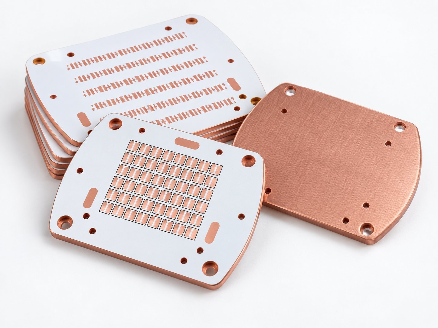
A heavy copper PCB uses thicker copper conductors to increase the cross-section available for power routing. It is also called a thick copper PCB.

Epec uses a 4–20 oz/ft² range for heavy copper. For purchasing, specify the copper weight and required finished thickness on each layer rather than relying on the label alone.

Specify the copper you need at the end of fabrication.

State the layer, nominal copper weight and any minimum finished thickness in micrometres. Keep base foil, finished conductor copper and plated-hole copper as separate requirements.

Electrical

More conductor cross-section

For the same trace length, width and temperature, increasing copper thickness reduces DC resistance. Current limits still depend on the resulting heat and the full connection path.

Thermal

Better lateral heat spreading

Thicker copper planes can spread heat across the board. Vias, interfaces, heat sinks and airflow determine how effectively that heat leaves the assembly.

Architecture

Power and control, planned together

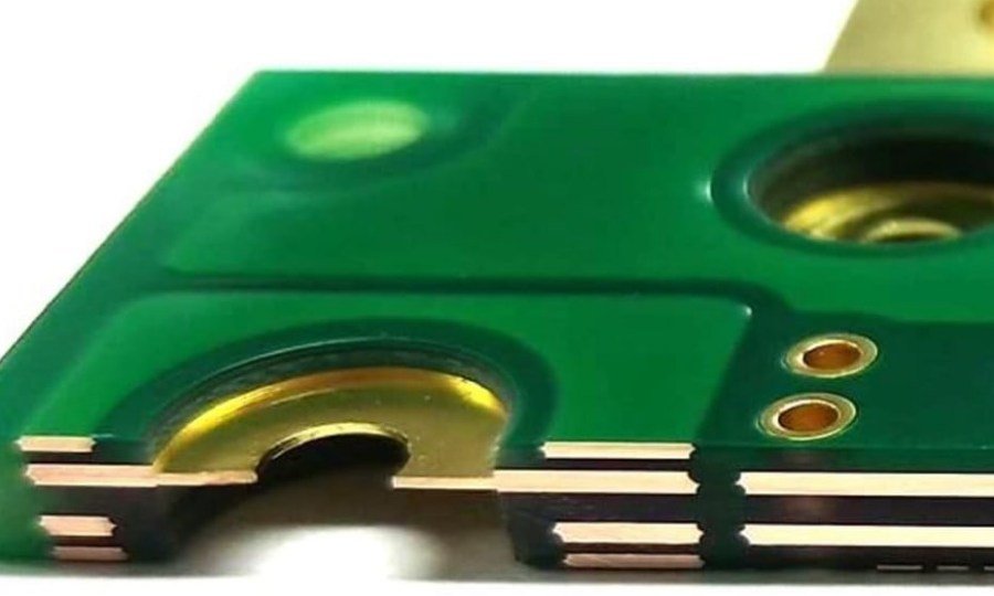
A reviewed stackup can combine different copper weights on different layers. Fine-pitch signal routing and heavy-current areas need compatible fabrication rules.
02 / Copper weight reference

Heavy copper PCB thickness, at a glance.

PCB copper weight is mass per unit area. The common rounded convention is 1 oz/ft² ≈ 35 µm. The table scales that convention; actual finished copper depends on foil tolerance, processing and plating.

Use these nominal values for comparison, then specify finished copper thickness and tolerances in your drawing.
Copper weightNominal thicknessIn millimetres
1 oz/ft²≈ 35 µm≈ 0.035 mm
2 oz/ft²≈ 70 µm≈ 0.070 mm
3 oz/ft²≈ 105 µm≈ 0.105 mm
4 oz/ft²≈ 140 µm≈ 0.140 mm
6 oz/ft²≈ 210 µm≈ 0.210 mm
8 oz/ft²≈ 280 µm≈ 0.280 mm
10 oz/ft²≈ 350 µm≈ 0.350 mm
12 oz/ft²≈ 420 µm≈ 0.420 mm

On narrow screens, scroll the table horizontally to view all columns.

A better drawing note: identify the relevant layer and required minimum finished copper explicitly. Agree the measurement method and tolerance before treating a nominal “4 oz” label as an acceptance criterion.

03 / Design for manufacturing

Design the whole current path—not just a thicker trace.

Use an early DFM review to resolve geometry, construction and assembly questions before freezing the layout. The checklist below is a starting point for that discussion.

01

Trace width and spacing

Do not reuse light-copper routing limits unchanged. Ask for layer-specific rules based on the base foil, finished target and etching or plating route. Check the narrowest part of the actual conductor profile.

02

Vias and current transitions

Review via arrays, plated barrels, pads, thermal spokes and connector neck-downs as part of the same current path. Specifying heavy surface copper does not define the copper in a hole barrel.

03

Stackup, resin fill and copper balance

Ask the fabricator to review prepreg selection, resin fill between tall conductors, dielectric thickness and copper distribution. Include the layer map in the design package rather than leaving the construction implicit.

04

Solder mask and surface finish

Identify copper steps, mask coverage needs, openings and exposed conductors. Select the finish with the assembly process and contact requirements in mind; agree any special acceptance checks.

05

Assembly and thermal reliefs

Large copper areas draw heat away from pads during soldering. Review the soldering profile and any thermal-relief pattern together, so a solderability improvement does not create an unreviewed current bottleneck.

06

Material and electrical insulation

Specify the material grade, assembly exposure and service environment. Review dielectric thickness, spacing and insulation requirements against the working voltage and applicable product rules—not copper weight alone.

Bring the operating conditions

What should a current-capacity review include?

  • Continuous current, peak current, pulse duration and duty cycle.
  • Trace geometry, finished copper and layer location.
  • Ambient temperature, allowable rise and nearby heat sources.
  • Vias, terminals, copper planes, enclosure and cooling conditions.

IPC-2152 addresses current-carrying capacity in printed-board design. Use a suitable engineering method, then validate the relevant load cases on the finished assembly.

Two different design decisions

Heavy copper is not the same as a copper-base PCB.

Heavy copper describes the circuit conductors. Metal-core or insulated metal substrate (IMS) describes a construction with a metal backing and an insulating layer beneath the circuitry. A copper base is not a substitute for specifying conductor copper.

Choose the architecture around the current route and the heat-removal path. Ask whether a conventional laminate, an IMS construction or another thermal solution best fits the project before finalizing the specification.

04 / Build the specification

Heavy copper PCB manufacturing requirements

A quotation should identify the copper, construction and verification scope together. Use this checklist to make your enquiry actionable.

Heavy-copper PCB requirements to include with your enquiry.
ItemProvide with your enquiryConfirm before release
Copper by layerBase and finished copper targets; minimum finished thickness where required.Per-layer copper map, tolerance and agreed measurement basis.
Stackup & board thicknessLayer count, stackup, overall thickness, dielectric spacing and tolerances.Material construction, lamination feasibility and copper balance.
Critical conductorsMinimum line/space, power nets, neck-downs and controlled-impedance features.Copper-dependent design rules and any changes needing approval.
Holes & viasFinished hole sizes, PTH/NPTH identification, via type and barrel requirements.Drill/plating route, annular rings, filling requirements and inspection scope.
Material & finishNamed laminate or performance requirement; solder mask and surface finish.Availability, approved alternatives and assembly compatibility.
Electrical & thermal inputsCurrent profile, voltage, ambient conditions, cooling and allowed temperature rise.Required engineering review and prototype or qualification load cases.
Acceptance & documentationApplicable IPC documents, class/revision, electrical test and report requirements.Sampling, evidence, acceptance criteria and traceability scope.
Quantity & deliveryPrototype/production quantities, drawing revision, destination and required date.Quoted scope, tooling, procurement and agreed delivery schedule.

On narrow screens, scroll the table horizontally to view all columns.

One approved specification, across all documents.

Keep the fabrication drawing, stackup, Gerber notes and purchase order consistent. Do not leave one document calling for base copper while another assumes the same number means minimum finished copper.

05 / Application context

Where heavy copper deserves a closer look

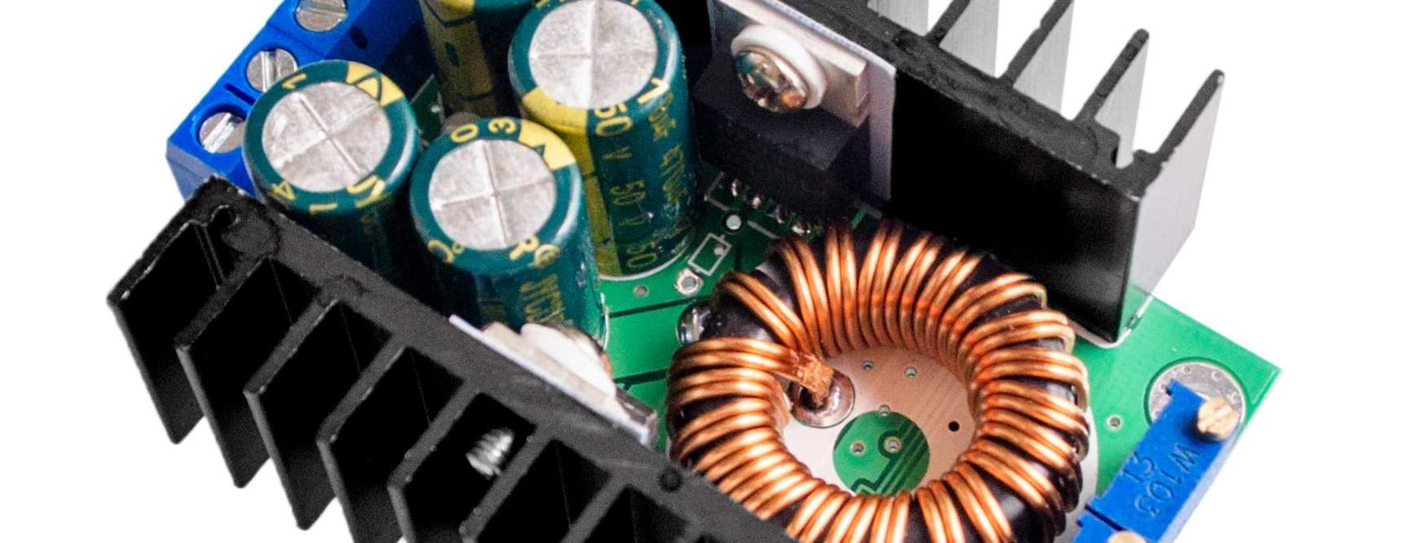
High-current power electronics are a common setting for heavy copper. Use the application to define the design inputs—not to assume a universal copper weight or current rating.
Power conversion & motor drives

Identify the switching stage, DC-link paths and power terminals. Review concentrated heat sources along with the board’s electrical connections.

EV charging & energy storage

Bring the charger or battery-system operating profile, peak loads and insulation requirements. Agree application-specific validation separately.

Renewable-energy power systems

For inverter and conversion projects, define thermal cycles, duty profile and enclosure cooling before comparing copper constructions.

Industrial power distribution

Map high-current routes, connector interfaces and installation constraints. Evaluate heavy copper against the needs of the complete system.

06 / Manufacturing review & verification

Agree how the construction will be verified.

Fabrication acceptance and application validation answer different questions. Establish both before the board enters production.

  1. 01 / Project review

    Review inputs

    Provide the design files, layer copper targets and operating profile. Identify any missing or conflicting requirements.

  2. 02 / Project review

    Agree the build

    Resolve stackup, materials, geometry changes and the required inspection scope before accepting a quotation.

  3. 03 / Project review

    Define the evidence

    Request the drawings, coupons, measurements and reports needed for the project’s acceptance criteria.

  4. 04 / Project review

    Validate & release

    Review prototype results against the relevant load cases. Control later material, copper and process changes.

Inspection planning

Ask for evidence that matches the requirement.

Conductor and plated-hole measurements
Microsections can reveal copper thickness and the internal construction at the sampled location. Agree coupon selection, measurement locations and acceptance criteria.
Dimensional, visual and electrical checks
Specify critical dimensions, continuity/isolation testing and required workmanship criteria. IPC-6012 addresses qualification and performance requirements for rigid printed boards; state the applicable class and revision.
Loaded thermal validation
Define the assembled-board test conditions, instrumentation and pass/fail limits. A copper-thickness result does not, on its own, validate operation under the intended load.

Agree the inspection methods, sampling and reports required for your copper structure and current-carrying design.

07 / Quotation planning

Compare complete builds, not just ounces.

Request a project-specific price and delivery schedule. A meaningful comparison keeps quantity, design revision and acceptance scope consistent.

Material & copper route

Identify the laminate, layer copper targets, allowed alternatives and any unusual procurement requirements.

Construction & geometry

Include stackup complexity, critical spacing, hole structures, panel requirements and the approved drawing revision.

Quantity & evidence

State the build quantity, required reports, qualification work, destination and requested date in the same enquiry.

08 / Frequently asked questions

Heavy copper PCB questions, answered.

Key distinctions for design notes, sourcing discussions and quotation requests.

Does heavy copper start at 3 oz or 4 oz?

Epec describes 4–20 oz/ft² as heavy copper. Specify the copper weight and required finished thickness on each layer instead of relying on the name.

How thick is 4 oz copper?

Using the common rounded convention of 35 µm per oz/ft², 4 oz corresponds to about 140 µm, or 0.140 mm. This nominal conversion does not establish the minimum finished thickness after processing.

How many amps can a heavy copper PCB carry?

There is no single current rating for a copper weight. The assessment needs the conductor geometry, layer location, temperature-rise limit, thermal surroundings and connection details. Review the actual design rather than using a universal amps-per-ounce figure.

Can different layers use different copper weights?

Different layer weights can be considered within a reviewed stackup. Specify each layer separately. Local thick and thin features on the same layer are a separate, process-specific question and should not be assumed from a mixed-weight stackup.

Can a heavy copper PCB use FR-4?

An FR-4 construction can be considered, but the exact grade and stackup must suit the project. Include assembly exposure, service conditions and electrical requirements in the material review. Request approval of the named material rather than specifying “FR-4” alone.

Is heavy copper the same as metal core or copper base?

No. Heavy copper refers to conductor thickness; an insulated metal substrate describes a metal-backed construction. The conductor requirement and the substrate architecture need separate specifications.

Can I keep the same fine-pitch layout when copper gets thicker?

Do not assume so. Thicker base copper generally calls for wider routing features, and the appropriate rules depend on the process. Review the critical footprints, neck-downs and clearances before changing copper weight.

What should I send for a heavy copper PCB quote?

Prepare Gerber or ODB++ data, drill files, a fabrication drawing, stackup and revision identifier. Add copper requirements by layer, quantities, operating conditions and acceptance criteria. For assembly, include the BOM and placement data. Agree a secure file-transfer route before sharing confidential designs.

Technical references & scope

Manufacturer and standards-body references support the engineering discussion. Their processes, capacity, certifications and delivery terms are not presented as GlobalWellPCB capabilities. All project limits and acceptance criteria require written agreement.

  1. Multi Circuit Boards — Thermal management for Printed Circuit BoardsTerminology and application context; supplier-specific capabilities are not adopted.
  2. Epec — Heavy copper PCB designAlternative terminology, current paths, mixed copper and fabrication concepts.
  3. Würth Elektronik — BASIC Design Rules (PDF)Copper-weight conversion and the distinction between base and finished copper.
  4. IPC — Design standards directoryIPC-2152, IPC-2221 and IPC-2222; agree the applicable document and revision.
  5. Würth Elektronik WEdirekt — Design Guide for PCBs from the online shop (PDF)Why base copper thickness affects routing rules; no generic minimum is copied.
  6. Epec — Heavy and extreme copper: holes, traces and spacingProcess-dependent geometry. Extreme-copper examples are not standard heavy-copper limits.
  7. Texas Instruments — Thermal design for power-tool motor drivesHeat spreading, thermal vias, heat sinks and airflow; application-specific figures are not generalized.
  8. Würth Elektronik — Technical Delivery Specification for PCBs (PDF)Construction and copper-thickness inspection methods, not a GlobalWellPCB test commitment.
  9. PCB Elegance — Thermal reliefThe solderability trade-off when pads connect to large copper areas.
  10. IPC — IPC-6012F qualification and performance scopeRigid-board qualification and performance scope; this does not assert that F is the latest revision.

Sources reviewed on 14 September 2026. Nominal conversions are for reference. Check the applicable controlled documentation for the build; references to IPC documents do not constitute certification or a claim that a named revision is the newest.

Scroll to Top