Flexible PCB Manufacturing
Flexible PCB manufacturing support for compact and moving assemblies. Send your polyimide FPC design, bend requirements, coverlay and stiffener details to discuss the right construction.
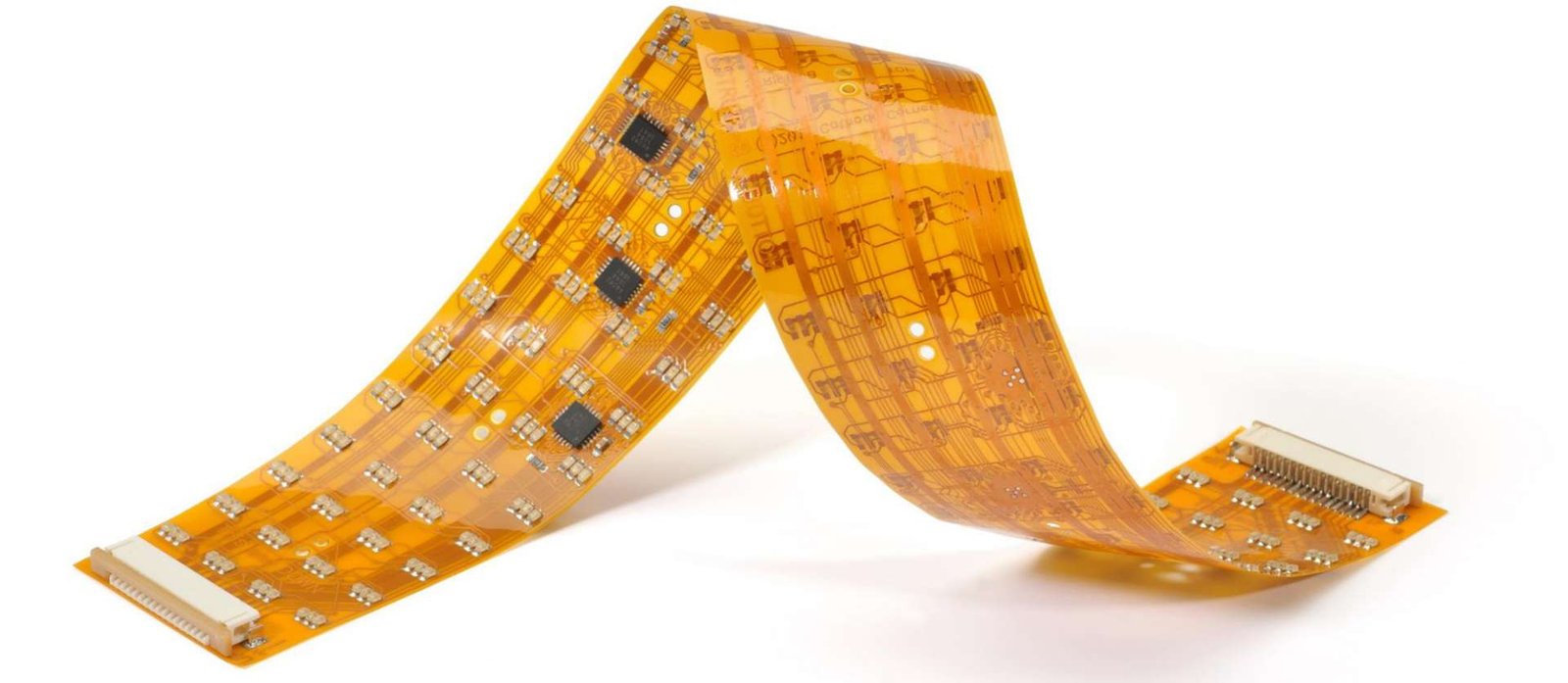
What is a Flexible PCB?
A flexible PCB is a printed circuit board manufactured on a bendable dielectric substrate, commonly polyimide. It is used to route electrical signals through folded, curved or space-constrained assemblies.
- Three-dimensional circuit routing
- Can reduce separate cables and connectors
- Movement and vibration performance require validation
- Thin interconnects for space-constrained assemblies
Core Components of a Flexible PCB
For related construction choices, review flex PCB stackup guide.
A flexible printed circuit board combines a dielectric film, conductors and protection layers. Adhesives and stiffeners depend on the chosen construction.
Base Substrate
Polyimide (PI), Polyester (PET), or LCP film providing flexibility and insulation.
Conductor
Rolled Annealed (RA) or Electrodeposited (ED) copper carrying electrical signals.
Bonding System
Adhesive-based or adhesiveless copper-clad construction; an adhesiveless laminate does not have a separate copper-to-film adhesive layer.
Coverlay
Polyimide film with adhesive protecting conductors from environmental exposure.
Substrate Materials Comparison
Compare flexible PCB materials by the exact laminate grade, assembly process, moisture exposure and bend duty. Film properties alone do not establish the operating limits of the finished flex circuit.
Polyimide (PI)
A common starting point for polyimide flex PCB designs. Match the laminate, copper, coverlay and bonding system to the assembly and mechanical requirements.
Polyester (PET)
An option for selected cost-sensitive flexible circuits. Confirm conductor technology and assembly temperature compatibility rather than substituting PET for a solderable PI construction.
Liquid Crystal Polymer (LCP)
An alternative to evaluate when moisture or high-frequency performance drives the specification. Manufacturing route and availability require confirmation.
Rolled Annealed vs Electrodeposited Copper
Copper foil selection affects mechanical performance. Rolled annealed (RA) copper is often considered for repeated bending, but a copper label alone does not establish a flex-cycle rating.
RA Copper
RA copper is commonly evaluated for demanding bend applications. Confirm the foil grade, thickness, grain orientation, plating in the bend zone and representative cycle testing.
ED Copper
Electrodeposited copper covers multiple foil grades. Suitability depends on ductility, construction and the specified bend duty; do not assume all ED foils have identical mechanical behavior.
Flex PCB Bend Radius Design
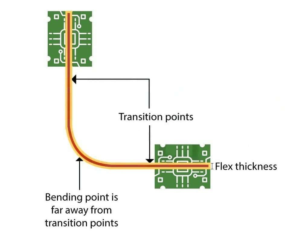
Minimum bend radius depends on the finished flex thickness, number of copper layers, copper type, bend direction, bend frequency and the required service life.
Define the Bend-Radius Requirement
The bend ratio relates the inside bend radius to the finished thickness of the flexible section. The acceptable ratio must be agreed for the actual stackup and motion profile.
r = k × tr: bend radius · t: flex thickness · k: agreed ratio- Identify whether the bend occurs during installation or throughout operation.
- Specify finished flex thickness, copper layers and the bend axis.
- Include bend angle, cycle target and environmental conditions.
- Validate the approved construction under representative conditions.
Example only: a 0.10 mm flex section and an assumed ratio of 10 give a 1.0 mm radius. This arithmetic example is not a recommended minimum. Keep vias, pads and rigid supports out of the active bend unless specifically qualified.
| Bend condition | Design information | Confirmation basis |
|---|---|---|
| Static installation bend | Installed shape, radius, angle and expected re-forming | Approved bend drawing and material construction |
| Repeated dynamic flex | Cycle target, motion speed, radius and environment | Representative mechanical and electrical testing |
| Multilayer flex | Copper-layer count, bonding and neutral-axis location | Construction-specific engineering review |
| Rigid-flex transition | Rigid edge, coverlay termination and keepout zones | Coordinated mechanical and fabrication drawings |
Supplier recommendations can differ by construction. Compare rigid-flex bend guidance with the approved project requirements; do not treat a generic ratio as an IPC acceptance rule.
On smaller screens, scroll this table horizontally to compare all columns.
Flex PCB Design Rules for Bend Reliability
Proper trace routing, pad geometry and copper distribution are essential for flex circuit reliability.
Recommended Practices
- Route conductors across the bend axis where practical.
- Use smooth transitions and avoid abrupt conductor-width changes in bend zones.
- Review copper distribution and stagger opposing traces where appropriate.
- Balance ground-plane continuity against mechanical flexibility.
- Review pad reinforcement, teardrops and strain relief.
Avoid These Practices
- Unqualified vias or plated holes in active bend zones.
- Sharp corners or stress concentrations in repeatedly bent conductors.
- Rigid supports ending directly in an active bend.
- Changing solid planes to mesh without an impedance and return-path review.
- Unsupported components or connectors near a flex transition.
Coverlay and Stiffeners for FPC Manufacturing
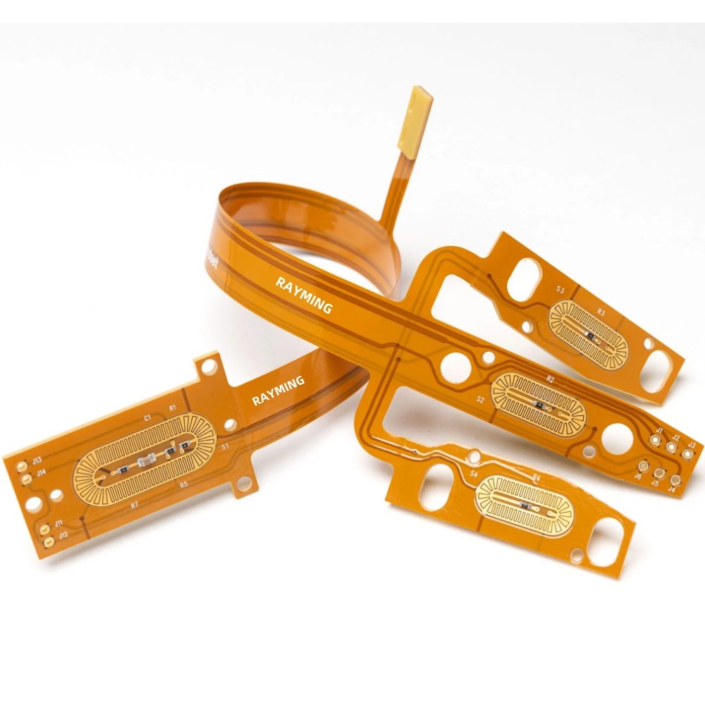
Coverlay protects conductors while leaving access to pads. Stiffeners support areas such as connectors or component zones, rather than increasing the electrical layer count.
Specify coverlay openings
Include pad access, opening dimensions, overlap and registration requirements. Coordinate coverlay with soldering, bonding and the installed bend position.
Document stiffener interfaces
State material, finished thickness, adhesive, location and which side of the FPC is supported. Keep the stiffener edge and associated strain outside the active bend where practical.
For a flex PCB prototype, use the same approved construction and bend conditions planned for validation. A prototype photograph alone is not evidence of production reliability.
Flexible PCB Manufacturing Requirements to Confirm
Prepare your flex PCB construction, bend conditions and inspection requirements for a quotation. We will confirm achievable dimensions and tolerances against your fabrication files.
| Requirement | Provide with your enquiry | What must be agreed |
|---|---|---|
| Layer count and thickness | Flex layer count and finished construction | Rigidized zones, bonding system and tolerances |
| Trace width and spacing | Critical geometry and copper thickness | Etching, plating and yield requirements |
| Drilled holes and vias | Finished dimensions, pads and layer connections | Registration, annular ring and bend keepouts |
| Coverlay | Openings, access pads and overlap | Process tolerance and minimum bridges |
| Stiffeners | Material, thickness, location and adhesive | Assembly support and connector fit |
| Impedance | Target, tolerance, reference layers and controlled nets | Approved stackup, geometry and test coupons |
| Prototype and production | Quantity, revision and qualification scope | Material availability, test plan and quoted schedule |
Technical parameters are project-dependent. Actual capability should be confirmed during DFM review.
On smaller screens, scroll this table horizontally to compare all columns.
Applicable IPC Standards
Include the IPC documents, product class and revision your order requires so we can confirm the applicable acceptance criteria for your flex PCB.
| Document | Review topic | Project use |
|---|---|---|
| IPC-2223 | Flexible-board design | Design requirements and construction review |
| IPC-6013 | Flexible-board qualification and performance | Specify class, revision and acceptance scope |
| IPC-4202 | Flexible base dielectrics | Approved base material specification |
| IPC-4203 | Adhesive-coated dielectric films | Coverlay and bonding-material specification |
| IPC-A-600 | Printed-board acceptability | Agreed visual acceptance criteria |
On smaller screens, scroll this table horizontally to compare all columns.
Static Flex vs Dynamic Flex
Static Flex
A static flex circuit is formed during installation and remains mostly stationary. The allowed radius and number of installation bends depend on its actual construction.
Typical applications include folded interconnects between rigid board sections, space-saving circuit routing, and three-dimensional assemblies.
Dynamic Flex
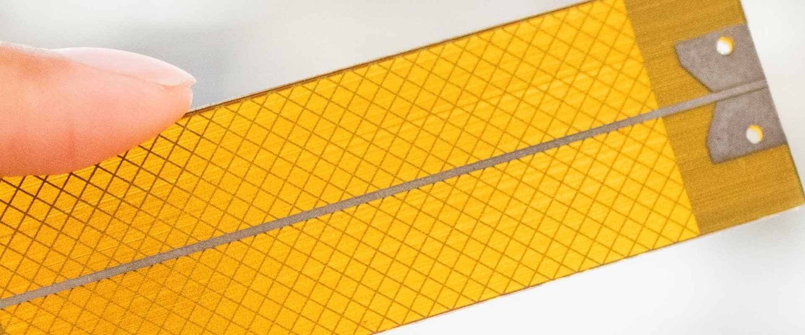
A dynamic flex circuit bends repeatedly during operation. Review foil grade, copper thickness, bend radius, trace geometry and cycle testing together; there is no universal cycle-life rating.
Typical applications include hinged displays, articulating robotic arms, moving scanner assemblies and folding consumer electronics.
Frequently Asked Questions
What is a flexible PCB?
A flexible PCB is a printed circuit board manufactured on a bendable dielectric substrate, commonly polyimide. It is used to route electrical signals through folded, curved or space-constrained assemblies.
What is the difference between static flex and dynamic flex?
Static flex is formed into a position during assembly and remains mostly stationary. Dynamic flex is designed to bend repeatedly during product operation and requires additional attention to copper type, thickness, bend radius and trace geometry.
Which material is normally selected for flexible PCB designs?
Polyimide is a common starting material for flexible PCB designs because it supports thin constructions, elevated assembly temperatures and repeated mechanical movement. PET and LCP may be considered when cost, temperature, moisture or high-frequency requirements call for a different material system.
What determines the minimum bend radius of a flex circuit?
Minimum bend radius depends on the finished flex thickness, number of copper layers, copper type, bend direction, bend frequency and the required service life. Dynamic applications generally need a larger bend radius than static formed flex.
Can components be assembled on a flexible PCB?
Yes. Components can be assembled on designated rigidized areas or supported component zones. Stiffeners, pad geometry, thermal conditions and the assembly process should be reviewed before production.
What files are needed for a flexible PCB quotation?
A quotation normally requires fabrication data, layer count, material preference, copper weight, finished thickness, surface finish, stiffener details, flex-zone drawings, quantity and any impedance, testing or assembly requirements.
What is the difference between flexible PCB and rigid-flex PCB?
A flexible PCB uses a flexible base and may include stiffeners or supported component zones. A rigid-flex PCB integrates rigid laminate sections and flexible interconnect regions in one board; a stiffened flex circuit is not automatically a rigid-flex construction.
Technical References and Scope
Explore the material and design references below to compare construction options. Ask us to confirm the selected material, processes and delivery requirements for your design.
- All Flex: rigid-flex construction and bend-design guidance
- All Flex: conductor geometry and fillet guidance
Send your material grade, construction, applicable standards and acceptance requirements with your enquiry so we can prepare a quotation for your board.