GlobalWellPCBPCB & PCBA Manufacturing
PCB Fabrication

Rigid PCB Capabilities

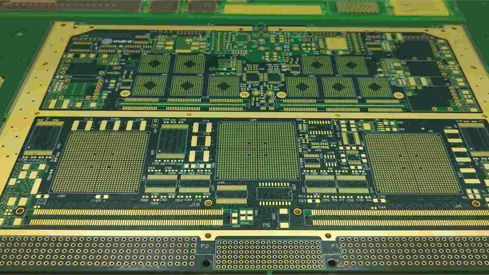
Review multilayer construction from the finished board inward: layer count, copper distribution, dielectric thickness, holes and controlled features. The specification register separates published limits from the conditions needed to build your particular board.

Panel of bare circuit boards with dense traces, component pads and board outlines
Multilayer PCB panel example. Illustrative example.
Capability register

Scope and conditions

Read each value together with its board type and review conditions.

68LMaximum layers
Rigid construction; approved stackup
85ozFinished copper
Rigid inner and outer limits reviewed separately
2.5/2.5milInner trace / space
Copper-dependent; outer layers differ

Published limits apply to their stated board type. Layer count, copper weight and minimum geometry require a combined engineering review.

Capability register

Rigid PCB specification register

These are individual rigid-board values. The final stackup and manufacturing drawing define the accepted combination.

On smaller screens, scroll within the table to see every column.

ParameterPublished capabilityApplies toReview conditions
Maximum layers68LRigid PCBRigid-board limit; material, thickness and via structure require review
Finished inner / outer copper85oz / 85ozRigid layers onlyReview the copper on each layer; minimum geometry cannot be assumed at maximum copper
Inner trace / space2.5/2.5milInner copper patternCopper thickness, local density and etch allowance
Outer trace / space3/3milOuter copper patternFinished copper, plating and solder-mask definition
Board thickness0.4–11.5mmFinished rigid boardStackup, tolerance and hole depth considered together
Minimum mechanical drill0.1mmMechanical drillingDistinguish drill-tool size from specified finished hole
Minimum laser drill0.075mmLaser-drilled structureDielectric depth, pad, layer span and fill requirements
Mechanical / laser aspect ratio20:1 / 1:1Respective hole processesNot interchangeable; confirm diameter and processed depth
Capability register

Finished board and process panel

A process-panel format includes manufacturing margins. It is not the finished-board outline.

On smaller screens, scroll within the table to see every column.

ParameterPublished capabilityApplies toReview conditions
Process panel formats600 × 770mm; 500 × 1200mmRigid process panelUsable area, tooling margins, material format and structure
Minimum finished board10 × 10mmIndividual rigid outlinePanelization and handling must be defined
Maximum finished board22.5 × 30inchIndividual rigid outlineConfirm material format, tooling and required tolerances
Contour tolerance±0.1mmRouted finished contourCritical datums and local features belong on the drawing
Thickness tolerance below 1.0mm±0.08mmRigid boards <1.0mmState finished nominal thickness and measurement requirements
Engineering review

Imaging and registration

Artwork must describe the intended copper geometry and its relationship to holes and board edges.

Send one controlled revision of the fabrication layers and drill files. Identify polarity, copper text, fiducials, alignment targets and any registration-sensitive areas in the fabrication drawing.

For fine geometry, review the actual layer and copper thickness. Inner and outer limits are different, and a local high-density area may need a different process allowance from the rest of the board.

Engineering review

Copper patterning and copper balance

Use the finished copper requirement to review etching and plating with the circuit pattern.

Layer-by-layer definition
State the required finished copper for every layer. Mark high-current regions, fine-pitch escape routing and isolated copper areas that may drive the review.
Controlled geometry
Identify whether a width is a nominal artwork dimension or a finished requirement. Include the permitted adjustment for impedance-controlled tracks.
Copper distribution
Provide plane clearances and keepouts as intended. Any proposed copper additions or manufacturing compensation require agreement where they affect the design.
Capability register

Solder mask capability

Mask opening and dam values apply to the mask process; they are not replacements for copper spacing rules.

On smaller screens, scroll within the table to see every column.

ParameterPublished capabilityApplies toReview conditions
Mask colors listedGreen, black, blue, red, white, purple, pink, yellow, matt black/green/blue, orange, clear or transparentRigid solder maskConfirm color, material and compatibility with the board and assembly
Minimum clearance1.5milRigid solder-mask clearanceOpening convention, registration and pad geometry
Minimum dam3milRigid solder maskFine-pitch pad spacing, finish and assembly process
Capability register

Legend and marking

Prioritize readable part identification without placing ink on exposed solderable surfaces.

On smaller screens, scroll within the table to see every column.

ParameterPublished capabilityApplies toReview conditions
Legend colorsWhite, black, red, yellowRigid legendChoose contrast against the selected mask
Minimum width / height4mil / 23milLegend featuresFont, local space and readable orientation
Marking controlDrawing-definedRevision and identificationState the exact content and permitted relocation areas
Documented project examples

Reference multilayer constructions

These examples describe individual structures in our project reference material. They do not establish a general maximum or guarantee the same combination for a new design.

28L thick multilayer

The reference records 28L HTG, 3.65mm board thickness, 15:1 aspect ratio, 3/4mil geometry and impedance control. Those values belong to that construction.

Individual engineering example; the combination is reviewed for each project.

24L backplane

A separate reference records a 24L backplane with press-fit holes and impedance control. Connector hole requirements must be specified for each new backplane.

Individual engineering example; the combination is reviewed for each project.

Engineering review

Files and checks for a rigid-board RFQ

Let the drawing identify the non-negotiable features.

Fabrication package
Gerber/ODB++ or equivalent data, drill files, outline, stackup, copper by layer, finish and solder-mask requirements.
Critical features
Flag press-fit holes, impedance nets, dimensional datums, slots, edge features and the required tolerance for each.
Acceptance records
Specify electrical test, impedance or cross-section records needed with the order. Resolve any proposed manufacturing adjustments before release.
RFQ checklist

Send the files that define your build

Include the drawing revision and acceptance requirements. The engineering review confirms the manufacturable combination before quotation.

PCB fabrication

  • Gerber or ODB++ fabrication data and the board outline
  • Layer stackup, material identity, finished copper and board thickness
  • Drill data, impedance targets, surface finish and inspection requirements
Request PCB quote

PCB assembly

  • PCB fabrication package and an itemized BOM with manufacturer part numbers
  • CPL / pick-and-place data, assembly drawings and component polarity
  • Component sourcing scope, programming files and the agreed test procedure
Request PCBA quote
Engineering FAQ

Questions before you quote

Does 68L apply to flex or rigid-flex?

No. It is the confirmed rigid-board maximum. Flex and rigid-flex have their own published limits and construction review.

Can 85oz copper use the minimum trace/space?

Do not assume that combination. State finished copper per layer and the actual geometry for an etch, plating and stackup review.

Is the process panel size the maximum finished PCB size?

No. The table lists them separately because manufacturing margins, material format and panel construction affect the usable area.

What should I specify for a small hole?

State whether the dimension is a drill-tool or finished-hole requirement, identify plated or non-plated status, tolerance and the layers it passes through.

Scroll to Top