GlobalWellPCBPCB & PCBA Manufacturing
PCB Design

PCB Design Services

Bring your circuit requirements, board layout and manufacturing files into one coordinated project. Share your starting point with GlobalWellPCB to define the design work, review stages and deliverables you need.
  • Circuit & schematic
  • Placement & routing
  • Manufacturing handoff
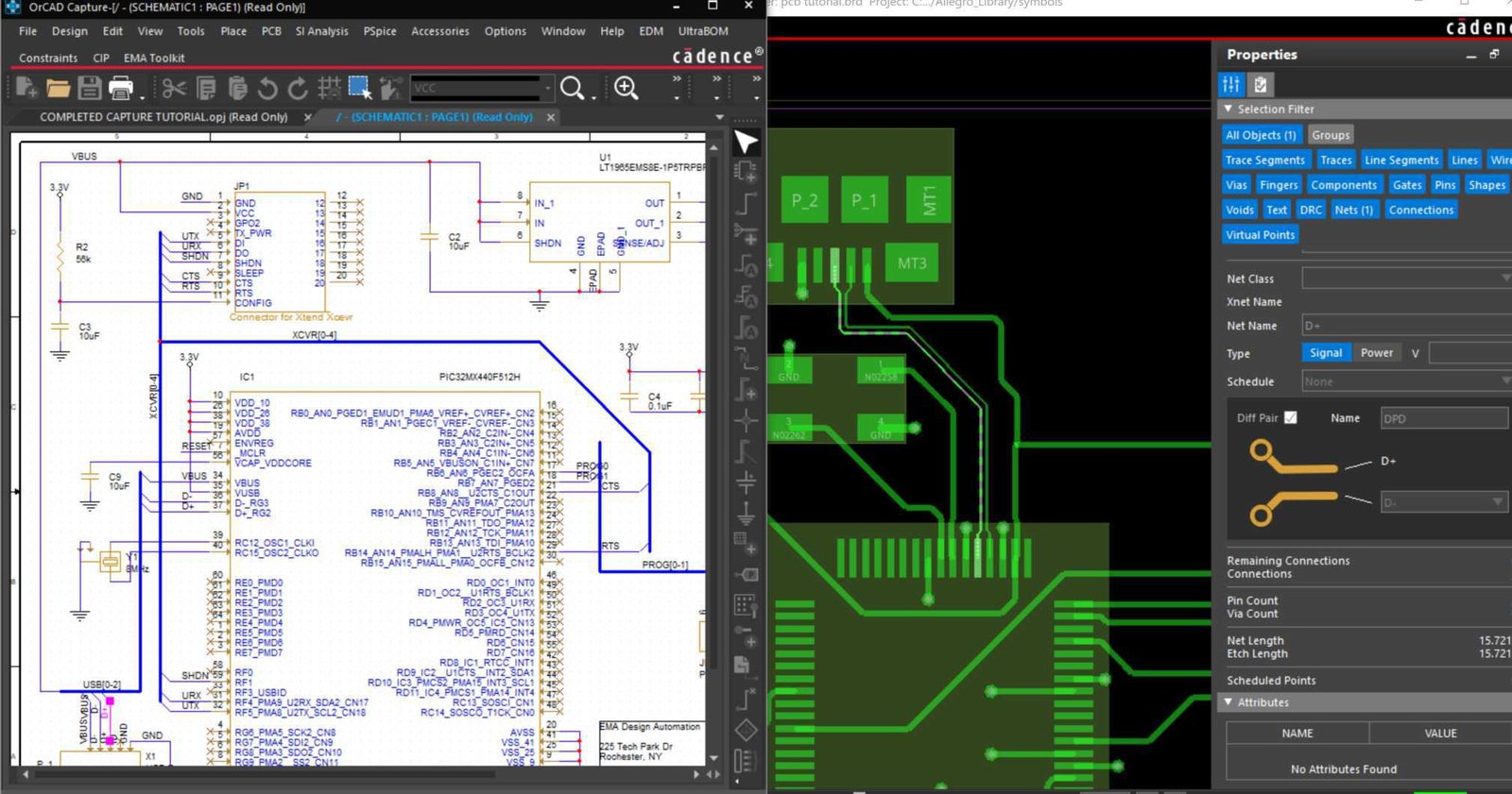
Illustration of a schematic and PCB layout shown side by side
Keep the schematic, layout and release files aligned.
Design scope

Plan the complete board design in one place.

Start with a new circuit, an approved schematic or an existing board that needs an update. The project scope connects the electrical, mechanical and production requirements.

  • Circuit & schematic design

    Organize the circuit functions, component references and electrical connections before placement begins.

    • Functional blocks, power inputs and interfaces
    • Symbols, connectivity and component records
    • Review findings and layout handoff notes
  • PCB layout & routing

    Turn the reviewed schematic into a board layout that fits the product and its manufacturing requirements.

    • Board outline, stackup and mechanical constraints
    • Component placement, footprints and keepouts
    • Routing, reference planes and critical nets
  • Design review & release

    Resolve rule-check findings and manufacturing questions before approving the release package.

    • Design rules and accepted exceptions
    • Fabrication, assembly and test-access review
    • Revision control and production file preparation
Your starting point

Choose the next step for your project.

Tell us what is already available and what needs to change. We can then define the work and review milestones for that revision.

  • A new board concept

    Share the required functions, power inputs, interfaces and mechanical envelope so the circuit and layout scope can be assessed.

  • An approved schematic

    Provide the schematic, BOM and board constraints to begin placement, routing and manufacturing preparation.

  • An existing design update

    Send the editable source, matching files and your change list. Identify substitutions, circuit updates and mechanical changes.

  • A layout ready for review

    Submit the current design rules, fabrication files and known issues to define the review and release requirements.

Working together

Review the design at each release stage.

Clear inputs and customer approvals keep the schematic, placement, routing and output files on the same revision.

  1. Define the scope

    Review the available files, required work, source formats and project constraints.

  2. Review the circuit

    Confirm connectivity, component records and questions that affect the board design.

  3. Plan & route

    Review the stackup and placement before completing the agreed routing work.

  4. Resolve findings

    Address design-rule, fabrication and assembly questions, then approve changes.

  5. Release the files

    Confirm the final revision and the fabrication and assembly outputs you require.

Files & deliverables

Start with your files. Agree the output package.

Send the information you already have and identify the revision. Required source formats and deliverables are confirmed when the work is scoped.

What to send

  • Circuit and component data

    Functional requirements, block diagram or schematic, netlist, BOM, relevant datasheets and available libraries.

  • Mechanical definition

    Board outline, dimensions, mounting holes, connector locations, keepouts and enclosure constraints.

  • Electrical and build requirements

    Power requirements, stackup preference, critical nets, impedance targets, intended quantities and assembly or test needs.

  • Existing project source

    Editable design files, the CAD tool and version, current manufacturing outputs and the changes or concerns to review.

What to request

  • Schematic and PCB source

    Agreed editable source formats and readable schematic drawings for your team.

  • Fabrication package

    Gerber or another agreed CAM format, drill files, board outline, stackup and fabrication drawing.

  • Assembly package

    A revision-aligned BOM, placement data and assembly drawings when assembly is included in the scope.

  • Review and release record

    Open questions, resolved findings, approved exceptions and revision notes.

Manufacturing handoff

Connect design decisions to the intended build.

Material, stackup, hole structure, copper, spacing and assembly constraints should be reviewed together before production files are released.
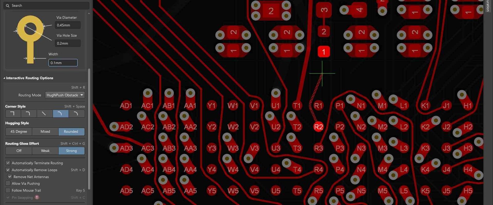
Illustration of PCB routing, pads and layout review panels
Review layout details against the agreed build requirements.
  • Fabrication requirements

    Confirm the material, finished construction, drill definitions, surface finish and controlled-impedance requirements for the actual board.

  • Assembly and test access

    Coordinate component footprints, polarity, spacing, placement outputs and the test-access requirements for your assembly plan.

  • Approval before release

    Keep the design source and output files aligned with the approved revision. Product performance verification remains part of your development plan.

Explore PCB manufacturing   ·   Explore PCB assembly

Your questions

Before you send your design files.

Include the questions that matter to your project so they can be considered when the scope and deliverables are agreed.

Can you start with a concept or block diagram?

A concept or block diagram can be a starting point for scope review. Include the required functions, power inputs, interfaces and mechanical constraints so the detailed work can be assessed.

Can you update an existing schematic or layout?

Send the editable source, matching schematic and board files, the current revision and your change list. Include any known circuit, fabrication or assembly concerns.

Which CAD tools and source formats can be used?

Tell us the CAD tool, version and library requirements your team uses. File compatibility and the editable output format are confirmed before the work begins.

Can I specify controlled impedance or critical routing?

Yes. Identify the critical nets, impedance targets, length requirements and proposed stackup where available. The routing requirements need confirmation for the actual board construction.

Will I receive fabrication and assembly files?

Agree the required outputs when the project is scoped. The package may include fabrication files, drill data, drawings, a BOM and placement data, according to the work and build requirements.

Does a design review confirm product performance?

Design-rule and manufacturing reviews address the checks in the agreed scope. Circuit function, signal performance, firmware and product compliance still need the appropriate engineering verification and product testing.

Discuss your project

What do you need to design, update or review?

Share your starting files, required changes and intended build. Define the design scope and release package with GlobalWellPCB.

Discuss Your PCB Design
Scroll to Top