Rigid PCB
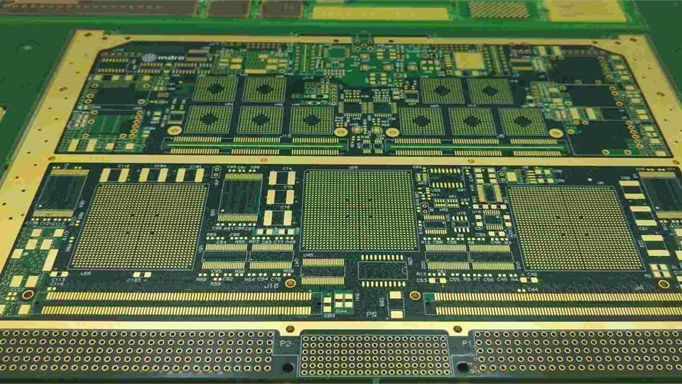
Up to 68L, with separate inner and outer geometry, copper, thickness and drill conditions.
View capabilityStart with the board or assembly your design needs, then check the specification, its scope and the files required for engineering review. Published limits describe individual capabilities; the stackup, copper, geometry and verification plan must work together.
Read each value together with its board type and review conditions.
Published limits apply to their stated board type. Layer count, copper weight and minimum geometry require a combined engineering review.
Choose a technical scope before comparing individual limits.
Up to 68L, with separate inner and outer geometry, copper, thickness and drill conditions.
View capabilityUp to 8L; confirm flexible thickness, copper, PI protection, stiffeners and bend requirements.
View capabilityUp to 36L; define rigid zones, flex layers, transitions and the installed shape.
View capabilityLaser microvias, blind and buried structures and a documented any-layer example; construction is reviewed from a via map.
View capabilityMaterial identity, hybrid stackups, impedance requirements and controlled via transitions.
View capabilityTwo different design routes: copper for current paths and a metal base for the thermal structure.
View capabilitySingle and double sided SMT/PTH, fine-pitch packages, panel handling and rework review.
View capabilityKeep bare-board verification, assembled-board inspection and functional test requirements explicit.
View capabilityUse the comparison to select a review path. A value in one column does not transfer to another construction.
On smaller screens, scroll within the table to see every column.
| Scope | Published reference | Key design dependency | RFQ package |
|---|---|---|---|
| Rigid PCB | 68L; 0.4–11.5mm board thickness | Copper, hole aspect ratio and stackup | Gerber/ODB++ or equivalent fabrication data, drill files and drawing |
| Flex PCB | 8L; 0.1–0.5mm board thickness | Bend zone, copper and stiffener boundaries | Fabrication data, flex stackup and bend/installation drawing |
| Rigid-flex PCB | 36L; 0.4–8mm board thickness | Layer count by region and rigid-flex transition | Region stackup, via map and installed assembly drawing |
| PCB assembly | 01005; BGA/Micro BGA 0.2mm pitch entry | Land pattern, component package, access and inspection | PCB data, BOM, CPL/pick-and-place and assembly drawing |
These references connect the capability table to the drawing and acceptance requirements.
Identify the exact core, prepreg and flexible material. Review substitutions before fabrication.
View capabilityDefine layer order, dielectric thickness, reference planes and impedance acceptance.
View capabilitySpecify finished holes, layer spans, via filling, backdrill and mechanical features.
View capabilitySelect the finish by assembly, contact and handling requirements; identify local areas on the drawing.
View capabilityThese examples describe individual structures in our project reference material. They do not establish a general maximum or guarantee the same combination for a new design.
A 28L HTG reference combines 3.65mm thickness, 15:1 aspect ratio and impedance control. It is a project example, separate from the general rigid limits.
Individual engineering example; the combination is reviewed for each project.
A 10L rigid-flex reference includes two flex layers and impedance in the flex area.
Individual engineering example; the combination is reviewed for each project.
A 6L reference combines Rogers4835 and Isola370HR with blind vias. Exact material identity and bonding details remain part of a new project review.
Individual engineering example; the combination is reviewed for each project.
Inspection answers a defined question; it should be specified alongside the product files.
Use the central quote form and identify PCB fabrication or PCB assembly in the request.
Send fabrication and drill data, the drawing, stackup, quantity and any controlled features. Identify the design revision.
View capabilityAdd the BOM, CPL/pick-and-place, assembly drawing, sourcing instructions and test requirements to the PCB package.
View capabilityMaximum layer count, maximum copper and minimum geometry are separate statements.
A design at one limit can change the usable range of another feature. Engineering review reconciles copper thickness with trace/space, hole depth with diameter, and material choice with lamination and impedance.
For quotation, identify the requirements that are essential and those that may be adjusted. A documented stackup and explicit acceptance criteria make that decision traceable.
Include the drawing revision and acceptance requirements. The engineering review confirms the manufacturable combination before quotation.
They are separate published limits. Submit the actual layer construction, finished copper and geometry so engineering can assess the combination.
Choose PCB fabrication for bare boards. For assembled boards, include the fabrication data plus BOM, CPL/pick-and-place, assembly instructions and the required test scope.
No. The examples document particular constructions. A new design needs its own material, stackup, via and acceptance review.