Aluminum PCB
A defined thermal path.A better-prepared build.
Bring your LED or power electronics project to GlobalWellPCB with a clear aluminum-base stackup, insulation requirement and mounting plan.
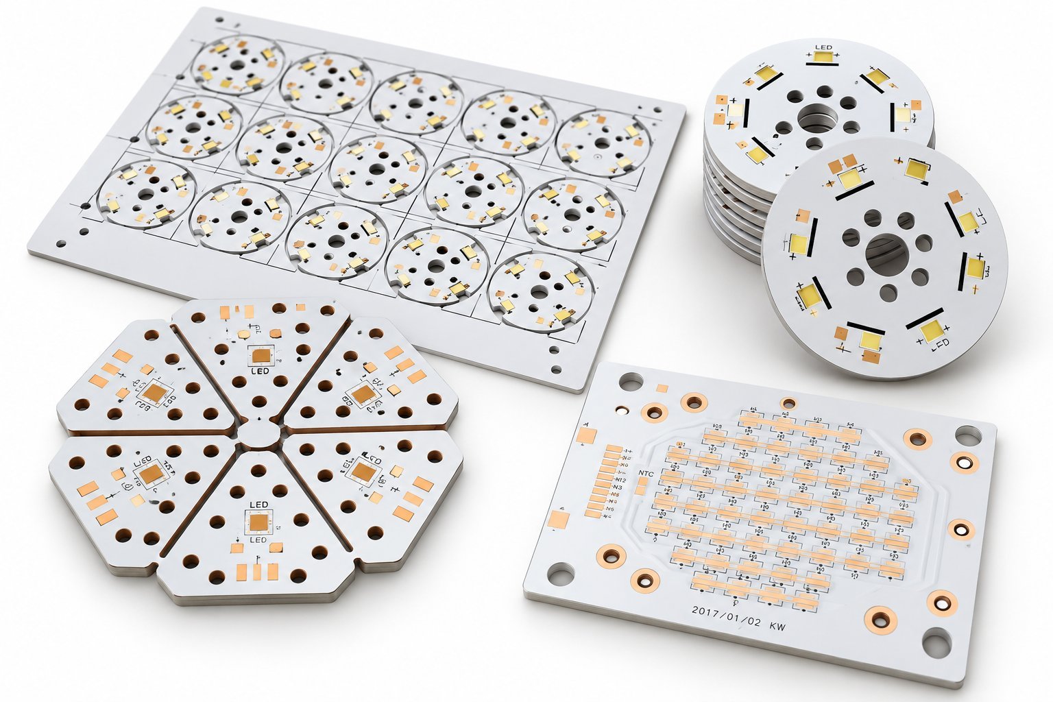
What is an aluminum PCB?
For related construction choices, review copper-base PCB, metal-core PCB, aluminum stackup guide.
An aluminum PCB uses a metal backing beneath an electrically insulating, thermally conductive dielectric and copper circuitry. The dielectric separates the circuit from the metal; the aluminum spreads heat toward the cooling interface.
The construction is also described as an aluminum-base PCB, an insulated metal substrate (IMS) or an aluminum metal-core PCB (MCPCB). The copper remains the circuit conductor—not the aluminum plate.
For an RFQ, define more than “aluminum PCB, 2 W/m·K.” Identify the laminate grade, dielectric thickness, copper, finished dimensions and operating conditions so the complete construction can be reviewed.
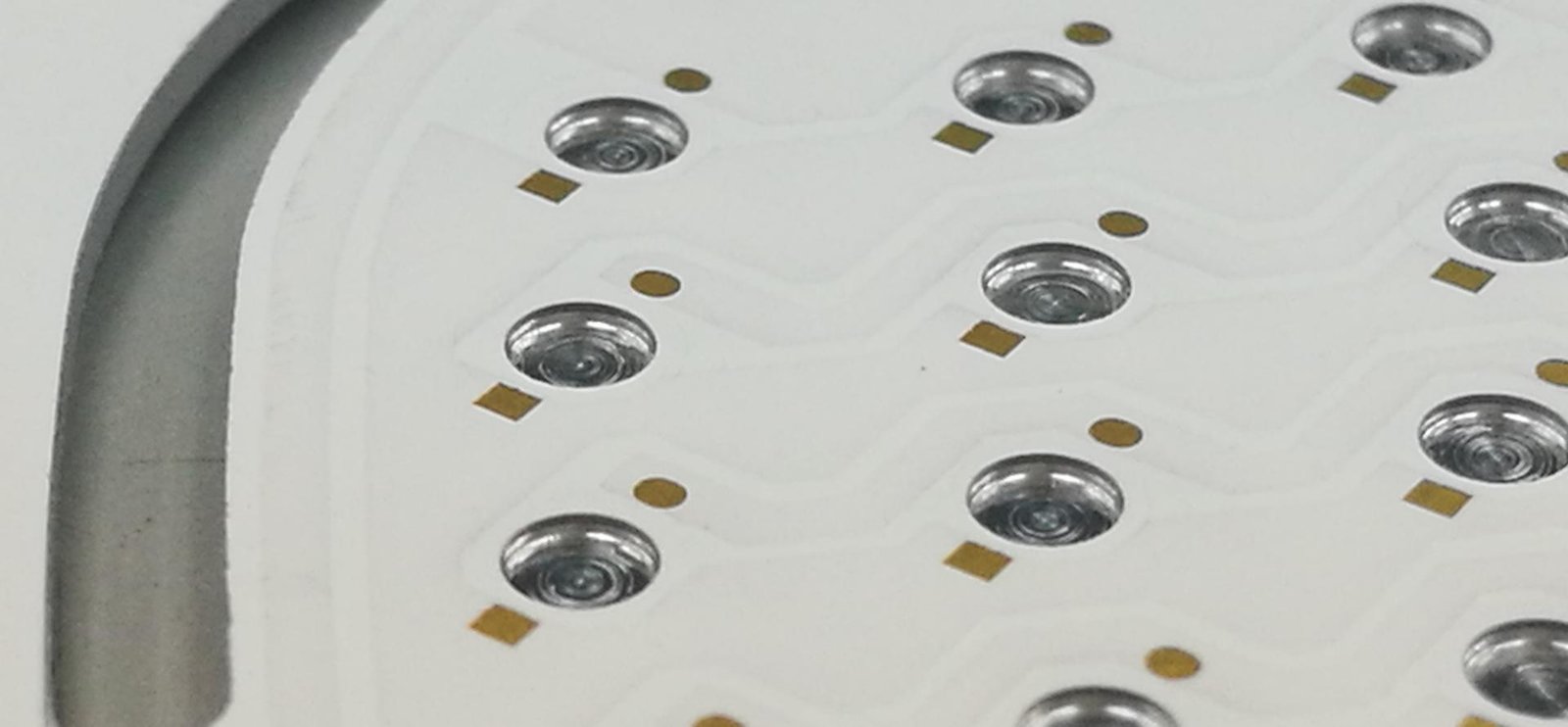
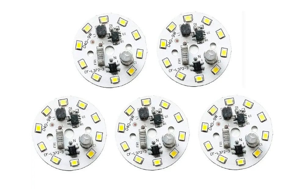
Each layer has a different job.
Start with the basic single-circuit-layer construction, then define any additional electrical or mechanical features.
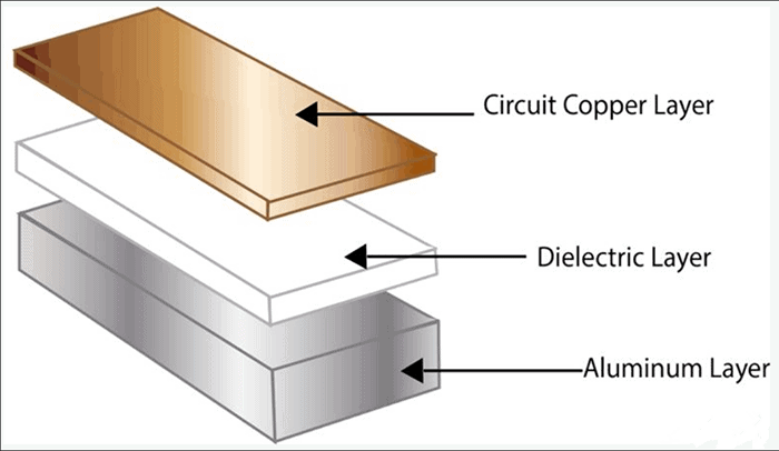
Copper circuitry
Routes electrical current and provides component pads. Specify copper in the required thickness convention, and distinguish starting foil from finished copper.
Thermally conductive dielectric
Bonds the circuit to the base while providing electrical insulation. Its thickness and thermal properties are central to the through-board heat path.
Aluminum base
Provides mechanical support and heat spreading. Name the alloy, temper, thickness and any critical machining or surface requirements.
Solder mask and pad finish are additional surface features. A white solder mask is not a substitute for specifying the thermal dielectric.
Specify the build.
Not just the base metal.
Prepare your aluminum PCB requirements with this checklist, then send your files to confirm manufacturing options and receive a quotation.
Scroll horizontally to view the full specification checklist.
| Specification | What to provide | What to confirm |
|---|---|---|
| Circuit construction | Single circuit layer, or a proposed multilayer/hybrid stackup. | Layer arrangement, interconnections and feasibility. |
| Dielectric | Supplier, grade, thickness, thermal property and test method. | Electrical isolation, operating temperature and approved substitutions. |
| Aluminum base | Alloy, temper, base thickness and total finished thickness. | Flatness, holes, edges and mounting-surface condition. |
| Circuit copper | Foil or finished copper thickness; current-path requirements. | Etched features, spacing and thermal constraints. |
| Mask & pad finish | Mask color and grade; preferred finish such as ENIG, lead-free HASL or OSP. | Assembly compatibility and finish availability for the construction. |
| Outline & delivery | Dimensions, holes, slots, panel drawing, quantity and revision. | Singulation, tolerances, inspection and requested reports. |
Use named material data.
TCLAD HT lists 2.2 W/m·K for the dielectric by ASTM D5470. Its separate “product thermal conductivity” value is 4.1 W/m·K under a different method. Those labels are not interchangeable.
Similarly, aluminum-alloy conductivity belongs to the metal layer, not to the assembled PCB or its insulating layer.
Baseplate thickness, dielectric thickness and total finished board thickness are three separate requirements. State all three where they are critical; do not assume a “1.6 mm board” defines each of them.
Published laminate examples for discussion
| Supplier / grade | Published conductivity | Listed dielectric thicknesses | Document context |
|---|---|---|---|
| TCLAD / HT | 2.2 W/m·K Dielectric value | 75, 100, 150, 225 µm | ASTM D5470 · HT TDS, Rev. 2023-D02-016 |
| Ventec / VT-4A2H | 2.2 W/m·K Datasheet conductivity | 75, 100, 125, 150 µm in the property table | ISO 22007-2 · TDS dated 24 August 2023 |
Confirm the current grade, construction and supply before ordering. Similar conductivity numbers do not establish equivalent insulation, temperature capability or measured thermal performance.
Look beyond the
W/m·K number.
A conductivity value alone does not describe the temperature rise through a particular thickness and area. Compare the complete thermal path, not just a material headline.
- Separate conductivity from resistance.
Conductivity k is expressed in W/m·K. Thermal resistance R is expressed in K/W (equivalently °C/W). An area-normalized value such as °C·cm²/W is a different quantity.
- Check what the datasheet actually measured.
Use the defined specimen and test method. Do not treat an ideal calculation as a replacement for supplier test results or finished-assembly measurements.
- Preserve the rest of the heat path.
For project review, include the heat-source footprint, dissipated heat, interface material, mounting pressure, heat sink and ambient conditions.
Dielectric thermal resistance estimator
Explore an ideal, steady-state, one-dimensional layer. The defaults are an illustrative example—not a recommended stackup.
R = t / (k × A) · ΔT = Q × R
Not a junction-temperature or heat-sink calculator. This model excludes heat spreading, package, solder, contact resistance and convection. Enter dielectric k, not aluminum k. Effective area must be justified; it is not automatically the whole board. Input bounds are tool limits only.
Is aluminum the right route?
Discuss the limiting requirement before committing to a substrate. The following are project-review questions, not automatic recommendations.
Aluminum-base IMS
Can the copper–dielectric–metal construction deliver the required thermal path while meeting insulation, routing and mechanical needs?
Review: heat path + mounting interfaceFR-4 construction
Can a conventional board, its copper arrangement and the proposed cooling system meet the same temperature target with a more suitable routing structure?
Review: routing + complete cooling designCopper-base IMS
Would changing the baseplate address the actual thermal or mechanical limitation? Compare the full construction, mass, machining and quotation—not the base alone.
Review: benefit + manufacturing trade-offsResolve the details
before production.
Send a mechanical drawing with your circuit files. Mark critical requirements explicitly rather than relying on a generic aluminum-PCB note.
Copper-to-edge and hole clearances
Clearance depends on the fabrication route, thickness and electrical requirements. Drilled, punched and routed features need different review.
Mounting holes and metal exposure
Identify insulated holes, exposed metal, fastener contact and any intentional chassis bond. Request an approved hole construction; do not assume an ordinary plated via can pass through the metal safely.
Flatness and the contact surface
Copper distribution, baseplate selection and machining can influence flatness. Define the mating area and its acceptable condition.
Panelization and separation
Part shape and singulation method affect material utilization and tooling. Review V-scoring, routing or punching with the intended order quantity.
Assembly and optical requirements
For PCBA, include the BOM, placement files, component thermal limits and profile requirements. For LED boards, specify any mask reflectance, color-stability or cleanliness acceptance criteria.
Electrical and thermal acceptance
Define continuity/isolation checks separately from circuit-to-base dielectric proof testing. Agree test conditions, production stage and reporting.
Do not use breakdown voltage as a working-voltage rating. Ask for an insulation review against the actual application, spacing rules and qualification requirements. A laminate value alone does not qualify the finished product.
Where the thermal path matters.
IMS materials are used in LED, power-conversion and motor-control applications. These are application examples, not customer case studies.
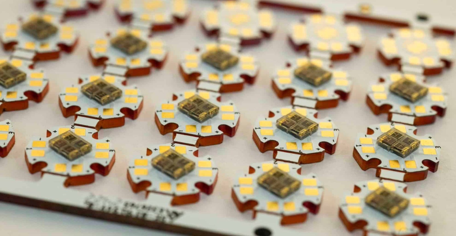
LED lighting modules
Bring the LED layout, heat-loss estimate, mounting interface and optical requirements into the same review.
Power conversion
Identify hot components, copper current paths, electrical isolation and the heat-sink attachment strategy.
Motor-control power stages
Specify power-stage dissipation, temperature cycling, fastener locations and critical mechanical interfaces.
Agree what will be verified.
Make acceptance criteria part of the quotation and approved drawing, rather than an assumption after fabrication.
Match the evidence to the requirement.
Request the records relevant to your product. Confirm available inspection methods, sampling and report delivery before release.
- Material and construction
- Grade, thicknesses, copper, approved substitutions and lot identification.
- Electrical insulation
- Define both circuit connectivity and circuit-to-metal insulation verification. These answer different questions.
- Mechanical and assembly interfaces
- Outline, hole positions, flatness, burr condition, finish and specified visual acceptance criteria.
- 01
Share the requirements
Provide drawings, fabrication data, quantities and the thermal/electrical brief.
- 02
Resolve open questions
Review the material, stackup, geometry, inspection scope and supply assumptions.
- 03
Approve the build
Confirm the revision, changes, acceptance criteria, price and schedule.
- 04
Review the agreed records
Check the delivered evidence against the approved order and retain the released configuration.
Aluminum PCB
FAQs
Clarify the terminology, material choices and quotation requirements before the next build.
Are aluminum PCB and metal-core PCB the same?
Aluminum PCB is one type of metal-core PCB. The broader category also includes other metal bases, such as copper. State the base material and the insulating construction explicitly.
What thermal conductivity should I specify?
Name the material, the property and its test method. For example, the TCLAD HT datasheet distinguishes dielectric conductivity from a separate product conductivity value. Neither is a complete board-to-ambient thermal resistance.
Can aluminum PCBs have more than one circuit layer?
Multilayer and hybrid IMS structures exist, but they require a defined stackup and interconnection approach. Send the proposed construction for review rather than assuming that a single-sided aluminum process supports it.
Does an aluminum PCB eliminate the need for a heat sink?
Do not assume it does. Evaluate the full heat-loss and temperature budget, including the metal base, contact interfaces and the final path to ambient. State the intended cooling arrangement in the RFQ.
Is aluminum PCB the same as alumina ceramic PCB?
No. Aluminum refers to the metallic element used here as a baseplate. Alumina is aluminum oxide, a ceramic. A ceramic-filled dielectric in an aluminum PCB does not make the baseplate an alumina substrate.
Can the aluminum base be used as electrical ground?
Only through an intentional, approved connection. The standard insulating layer separates the copper circuit from the metal base. Define grounding, mounting hardware and isolation requirements together.
Is Tg the maximum continuous operating temperature?
No. Tg, operating-temperature ratings and solder-process limits are different properties. Check the exact material documentation and the operating limits of the complete assembly.
What do you need for an aluminum PCB quotation?
Provide fabrication and drill data, the mechanical drawing, dimensions, quantity, revision, desired stackup and finish. Add thermal/insulation requirements and required reports; include the BOM and placement files when assembly is requested.
Technical references
- [1] TCLAD — IMS construction and application overview
- [2] Ventec — VT-4A2H material datasheet
- [3] TCLAD — HT dielectric datasheet (PDF)
- [4] TCLAD — Thermal Clad dielectric selection
- [5] TCLAD — IMS fabrication and finishing information
- [6] TCLAD — Tools for an Optimal Design (PDF)
Research checked 14 September 2026. Supplier material values and general process descriptions are not GlobalWellPCB capability guarantees. Material supply, approved construction, testing, price and lead time must be confirmed for each order. Product names belong to their respective owners; no authorized-distributor relationship is implied.