GlobalWellPCBPCB & PCBA Manufacturing
PCB Manufacturing

Advanced PCB Manufacturing Services

Get bare PCBs for prototypes and production, with support for materials, stackups and design questions before fabrication. Send your files to discuss the board construction and inspection your project needs.
Prototype to ProductionMultilayer & HDISpecialty MaterialsEngineering Review
Start your project

Send the Data That Defines Your PCB Build.

Share your fabrication data, construction requirements and critical features for a manufacturing review.

PCB Design Files

Package Gerber or ODB++ and drill files in a ZIP; add the stackup and fabrication drawing.

You can describe the requirements even if your files are still being prepared. Include quantities and target dates in your notes, if available.

Project enquiry

Add your contact details, requirements and available files.

Drag & Drop Files, Choose Files to Upload You can upload up to 5 files.
Package Gerber or ODB++ and drill files in a ZIP; add the stackup and fabrication drawing. ZIP, PDF, CSV, XLS/XLSX, TXT, JPG/PNG. Up to 5 files, 10 MB each. Contact us before uploading files that require an NDA.

Need an NDA? Contact us before uploading confidential design files.

Manufacturing Overview

A manufacturing route built around your design requirements.

PCB sourcing decisions depend on more than board type. Material behavior, stackup, copper distribution, hole structure, surface finish and inspection scope must work together. GlobalWellPCB reviews these inputs as one manufacturing package before production release.

Find the board type that fits your design, then send your fabrication files and requirements for a quotation.
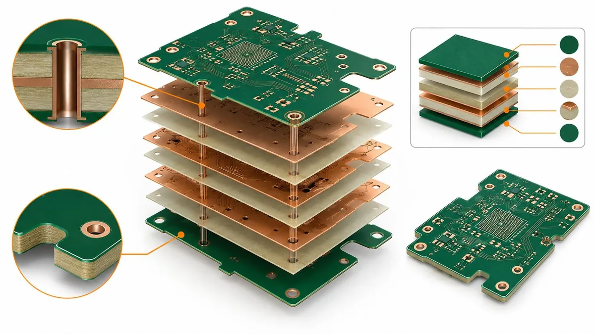
Exploded multilayer PCB showing copper layers, dielectric materials and plated through-holes.
Multilayer PCB stackup and plated through-hole structure. Illustrative diagram.
01

Prototype & Production

Plan early builds and later production requirements through one documented technical path.

02

DFM Review

Identify file, stackup, spacing and process risks before the board enters fabrication.

03

Material Alignment

Confirm the substrate and finish against electrical, thermal and assembly needs.

04

Verification Scope

Define inspection, electrical test and reporting requirements for the specific project.

PCB Fabrication

PCB Manufacturing
Capabilities

Explore our PCB fabrication specifications, material options and inspection methods for your next project.

ParameterManufacturing Capability
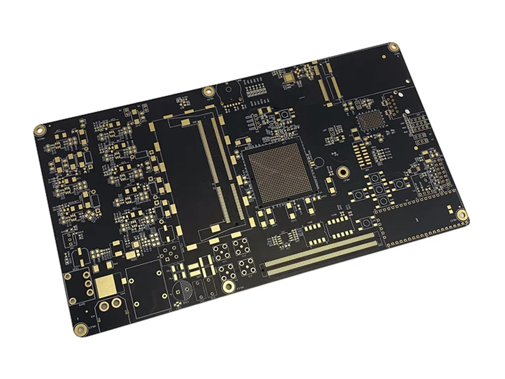
PCB TypesRigid, flexible and rigid-flex PCBs; HDI, high-frequency, controlled-impedance and metal-core constructions.
Layer CountRigid PCB: up to 68 layersFlex PCB: up to 8 layersRigid-flex PCB: up to 36 layers
Board ThicknessRigid PCB: 0.4–11.5 mmFlex PCB: 0.1–0.5 mmRigid-flex PCB: 0.4–8.0 mmFor boards below 1.0 mm: rigid / rigid-flex ±0.08 mm; flex ±0.05 mm.
Board DimensionsFinished board size and panel format are confirmed from your board outline and panel requirements.
Copper ThicknessRigid PCB: up to 85 oz, inner and outer layersFlex PCB: up to 2 oz, inner and outer layersRigid-flex PCB: up to 6 oz inner / 3 oz outer
Trace Width / SpacingRigid PCB inner layers: 2.5 / 2.5 mil minimumRigid PCB outer layers: 3 / 3 mil minimumMinimum features depend on copper weight and the selected stackup.
Drilling & Via StructuresRigid PCB mechanical drilling: down to 0.10 mmRigid PCB laser drilling: down to 0.075 mmBlind / buried vias, via-in-pad and backdrilling. Via filling and plating requirements are confirmed per project.
MaterialsFR-4, high-Tg, RF and low-loss laminates; flexible laminates and aluminium- / copper-base materials.Specify the laminate family, grade and acceptable alternatives.
Surface FinishesLead-free HASL, ENIG, hard gold, ENEPIG, OSP, immersion tin and immersion silver.
Controlled ImpedanceRigid PCB: ±5 Ω at ≤50 Ω; ±7% above 50 ΩFlex / rigid-flex: ±5 Ω at ≤50 Ω; ±10% above 50 ΩSingle-ended or differential. Confirm the stackup, test coupon and measurement scope.
Inspection & TestingAOI, electrical and flying-probe testing; visual and dimensional inspection.Test coverage, X-Ray applicability and required reports are agreed for the project.

Capability limits depend on board construction, materials and the selected process combination. Layer count, copper weight and minimum features are reviewed together for each build.

Ready to Discuss Your PCB Project?

Send your Gerber files, drill data, order quantity and fabrication requirements. Include any specified materials, impedance targets or inspection requirements.

Request a PCB Quote
PCB Types

Explore PCB Solutions for Your Needs

Explore PCB types by material, construction and design needs, with guidance on the files to send for a quote.
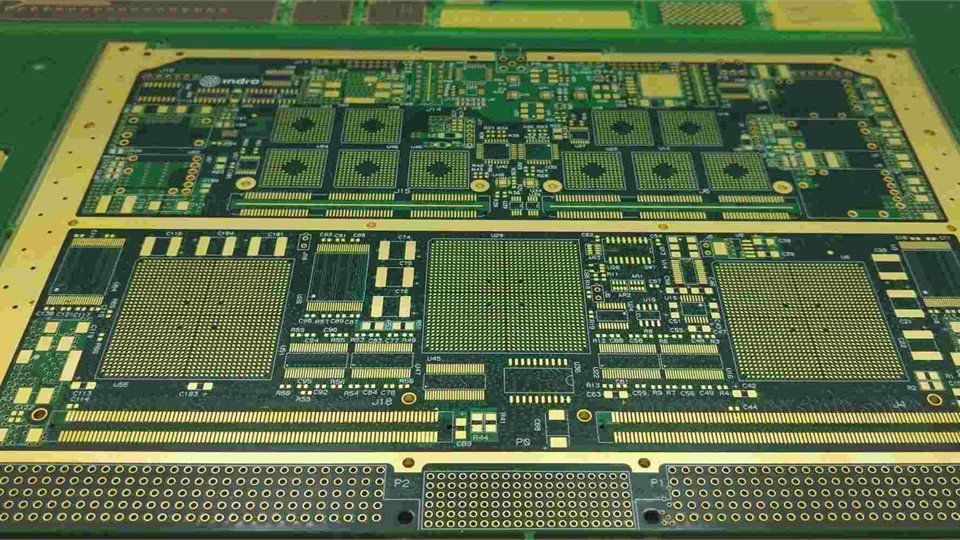
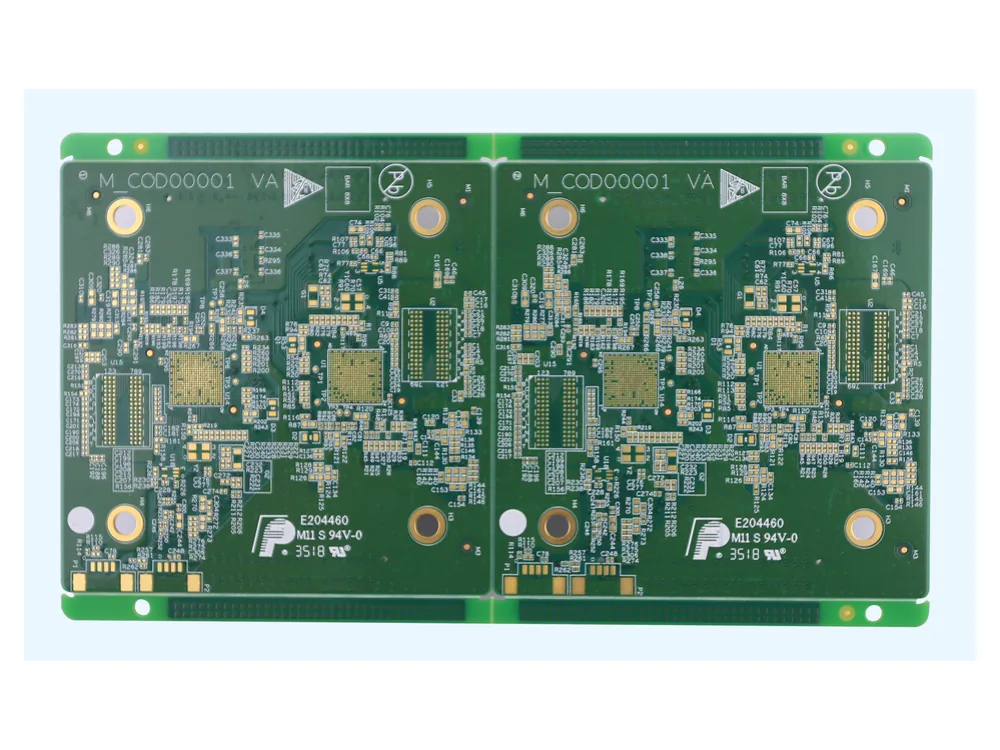
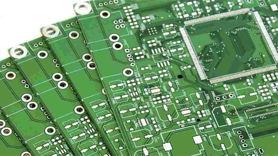
Multilayer PCB

Stackup planning, lamination, impedance and interlayer registration for complex rigid boards.
StackupImpedance
Explore capability

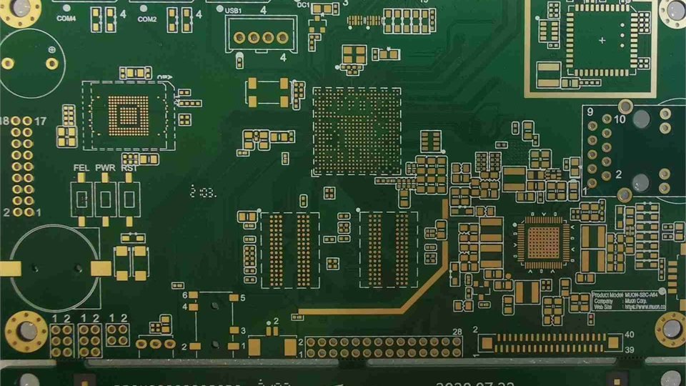
HDI PCB

Microvias, blind and buried vias, via-in-pad and dense interconnect structures.
MicroviaFine Features
Explore capability

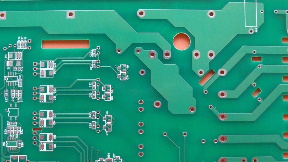
Heavy Copper PCB

Copper distribution, etching allowances and thermal paths for high-current designs.
High CurrentThermal
Explore capability

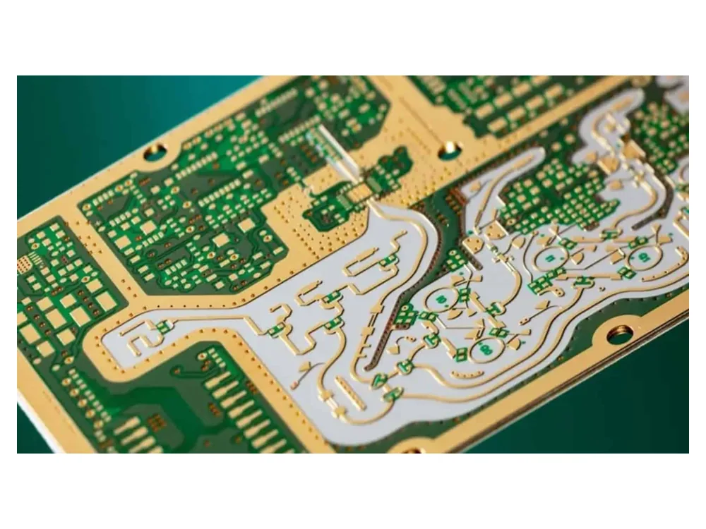
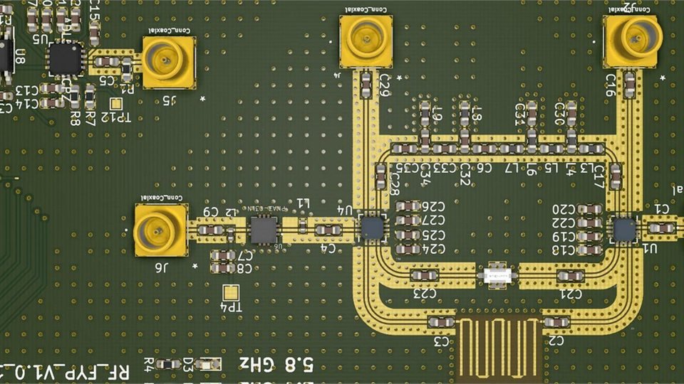
High-Frequency PCB

Low-loss materials, controlled impedance and hybrid construction for RF and microwave designs.
Low LossRF
Explore capability

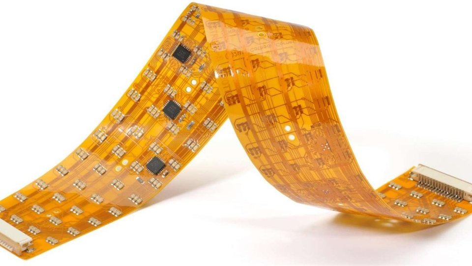
Flexible PCB

Polyimide circuits with coverlay, stiffeners and bend-area considerations.
PolyimideBend Area
Explore capability

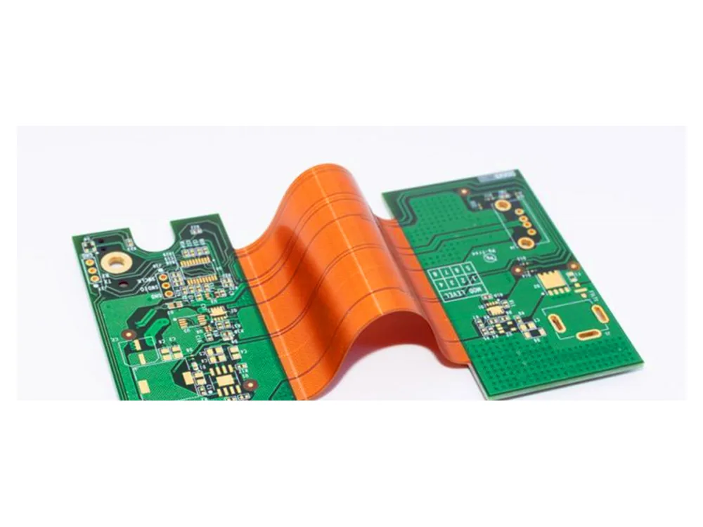
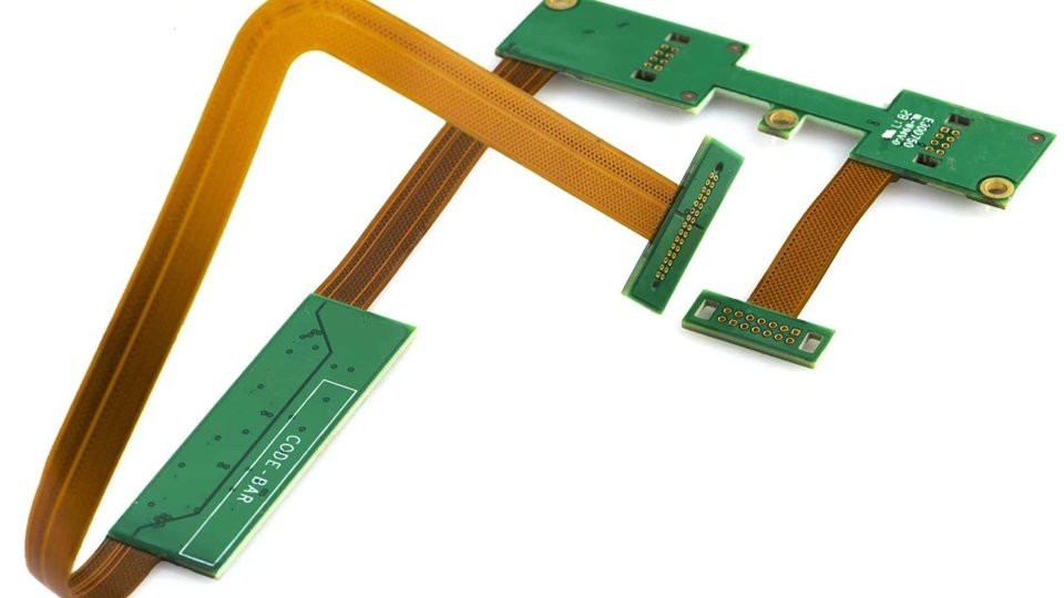
Rigid-Flex PCB

Rigid and flexible sections coordinated through one stackup and transition design.
TransitionStackup
Explore capability

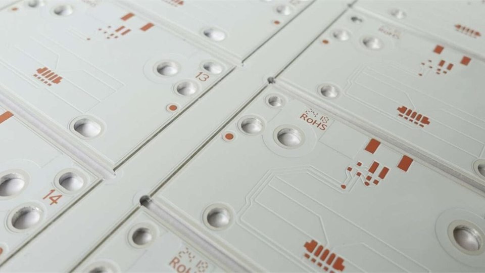
Metal-Core PCB

Aluminum or copper-base constructions designed around insulation and thermal transfer.
Metal BaseHeat Path
Explore capability

PCB Prototype

Fabrication support for engineering validation before the design moves toward production.

ValidationDFM
Explore capability
Advanced PCB Technologies

Organize complexity by its manufacturing risk.

Choose a technology below to review the design inputs and manufacturing considerations for your board.

HDI & Microvia Structures

Coordinate via type, sequential build-up, capture pads, plating and reliability requirements.

  • Review laser microvia and blind/buried-via definitions.
  • Confirm via-in-pad filling and surface requirements.
  • Provide stackup and interconnect intent with the RFQ.
Open HDI capability

High-Frequency & Low-Loss PCB

Align laminate selection, copper profile, stackup and impedance with signal-performance needs.

  • Identify the required material or electrical target.
  • Document controlled-impedance structures.
  • Review hybrid-lamination and mechanical constraints.
Open RF capability

Heavy Copper & High-Current PCB

Balance copper weight, conductor geometry, hole copper and heat flow across the finished board.

  • Share current and thermal design requirements.
  • Review etching allowances and spacing.
  • Confirm terminals, slots and mechanical interfaces.
Open heavy-copper capability

Flex & Rigid-Flex Construction

Define rigid, flexible and transition zones as one manufacturable stackup.

  • Mark dynamic and static bend regions.
  • Specify coverlay, stiffener and shielding needs.
  • Review conductor routing through transition areas.
Open rigid-flex capability

PCB Materials &
Surface Finishes

The board material forms the base of your PCB. The surface finish protects exposed copper pads and supports assembly or electrical contact.

PCB Materials

Choose the base material for your signal, temperature, flexibility and heat-management needs.

MaterialTypical Use & Options
Standard FR-4General-purpose rigid PCBs for control, industrial and consumer electronics.
High-Tg FR-4Projects with higher assembly-temperature requirements. Confirm the grade against the board's thermal requirements.
RF & High-Speed LaminatesRF, microwave or high-speed designs. Options include Rogers, Taconic, Arlon, Nelco, Isola, Megtron and PTFE; confirm the required grade.
Polyimide Flex MaterialsFlexible circuits and the flexible areas of rigid-flex boards.
Metal-Core MaterialsAluminum- or copper-base boards for LED lighting, power electronics and heat-management needs.

Surface Finishes

Choose the finish on exposed copper pads for soldering, wire bonding or contact wear.

Surface FinishTypical Use
Lead-Free HASLHot Air Solder LevelingGeneral soldered assemblies; review suitability when pad flatness is critical.
ENIGElectroless Nickel / Immersion GoldA flat surface for fine-pitch pads and soldered components.
Hard GoldElectroplated GoldGold fingers and contacts that need resistance to repeated wear.
ENEPIGElectroless Nickel / Electroless Palladium / Immersion GoldSoldering and wire-bonding projects; confirm the bonding process before selection.
OSPOrganic Solderability PreservativeAn organic coating that preserves copper solderability. Review assembly cycles and handling.
Immersion TinA flat tin surface for soldered assemblies; review assembly and storage requirements.
Immersion SilverA flat silver surface for soldered assemblies; review handling and storage conditions.

Exact laminate grades and finish specifications are confirmed for your board design and assembly requirements.

Need Help Choosing a Material or Finish?

Send your board files, operating requirements and assembly details. Include a preferred material or finish if you have one.

Request a PCB Quote

PCB Prototype
to Production

Follow the key steps from design-file review and prototype evaluation to production release and shipment preparation.

StageWhat Happens
01RFQ & Design FilesSend fabrication data, drawings, quantity and critical technical requirements.
02Engineering ReviewReview manufacturability, stackup, materials, vias and impedance requirements.
03Prototype BuildBuild the agreed prototype configuration for technical evaluation.
04Prototype VerificationComplete the agreed inspection and electrical testing for the prototype.
05Sample ReviewRecord sample approval, observations and any required design changes.
06Production ReleaseConfirm the production file revision, approved changes and manufacturing requirements.
07Final InspectionCheck the completed production lot against the agreed documentation and test scope.
08Delivery PreparationPrepare the finished boards and agreed project records for shipment.

The exact route and inspection scope depend on the board design and agreed project requirements.

Start with Your PCB Design Files

Send your fabrication data, drawings, quantity and critical requirements to begin the project review.

Request a PCB Quote
Manufacturing Process

A controlled path from material preparation to final inspection.

The exact route varies with the board construction. These stages provide a clear overview without replacing the project traveler or approved process documentation.

Material Preparation
Inner-Layer Imaging
Etching
Inner-Layer AOI
Lamination
Drilling
Copper Plating
Solder Mask
Surface Finish
Profiling
Electrical Test
Final Inspection

PCB Production in Pictures

Selected fabrication and inspection stages from sheet cutting to electrical testing. The production route varies with the approved board construction.

01–03

Sheet Cutting · Imaging · Lamination

PCB production steps 01–03: Sheet Cutting, Imaging, Lamination. Step labels appear above the equipment photographs.
04–06

Drilling · Plating · AOI

PCB production steps 04–06: Drilling, Plating, AOI. Step labels appear above the equipment photographs.
07–09

Solder Mask · Legend · Surface Treatment

PCB production steps 07–09: Solder Mask, Legend, Surface Treatment. Step labels appear above the equipment photographs.
10–12

CNC Routing · V-Cut · Electrical Test / TDR

PCB production steps 10–12: CNC Routing, V-Cut, Electrical Test / TDR. Step labels appear above the equipment photographs.
Quality, Equipment & Facility

Align inspection and testing with your board requirements.

Discuss inspection methods, test coverage and reporting requirements for your PCB project.

  • DFM and file reviewCheck construction and documentation before production release.
  • In-process inspectionApply inspection at the stages defined by the manufacturing route.
  • AOIReview patterned layers for relevant visual defects.
  • Electrical testingConfirm the project-specific continuity and isolation test scope.
  • Final inspectionReview dimensions, workmanship and agreed documentation before shipment.
Explore quality control
Application Areas

Review the board against its operating environment.

Explore board requirements for your application. Include any industry qualification or supplier-approval requirements with your enquiry.

01

Telecommunications

Signal integrity, low-loss materials, stackup and impedance requirements.

02

Industrial Electronics

Construction, temperature, power and service-environment considerations.

03

Power Electronics

Copper weight, current paths, spacing and thermal-management needs.

04

Automotive Electronics

Project-specific material, reliability, documentation and validation requirements.

05

Medical Electronics

Documentation, traceability and verification requirements defined by the customer.

06

Aerospace & RF Systems

Special materials, RF performance and project-specific acceptance requirements.

07

Consumer Electronics

Compact structures, form-factor constraints and production transition planning.

08

Robotics & Automation

Mixed signal, control, power and mechanical-interface considerations.

Engineering Resources

Prepare a clearer PCB manufacturing package.

Find guidance on materials, stackups, tolerances and manufacturing files before requesting a PCB quote.

FAQ

Before requesting a PCB quote.

Find answers about quotation files, material selection, testing and delivery planning.

What files are required for a PCB quotation?

Provide Gerber or ODB++ fabrication data, NC drill files, a board outline and available drawings. Include quantities, material, thickness, copper weight, surface finish, impedance and test requirements where applicable.

What information is needed for an HDI PCB?

Include the complete stackup, microvia and blind/buried-via definitions, sequential build-up intent, via-in-pad requirements and any controlled-impedance structures.

How should controlled impedance be specified?

Identify each impedance target, tolerance, referenced layers and trace structures. Share the proposed stackup when available so material and geometry can be reviewed together.

Which PCB materials are available?

The page groups common FR-4, high-Tg, RF, flexible, metal-core and ceramic material families. Exact grades and availability must be confirmed against the approved material list for the project.

Which surface finish should be selected?

The choice depends on assembly, flatness, contact wear, storage, wire bonding and signal requirements. Share the end-use conditions so the options can be reviewed.

Can prototype and production requirements be reviewed together?

Yes. Providing both quantity stages and the intended production requirements helps keep prototype decisions aligned with later releases, subject to project review.

What testing options are available?

Testing is confirmed for each project. The review should define electrical-test coverage, inspection stages, reporting needs and any additional verification required by the customer.

How are special materials and complex stackups evaluated?

Engineering review considers the laminate, copper, finished thickness, lamination route, hole structure, impedance and mechanical requirements as one construction.

Scroll to Top